In my previous post, I showed my design of a semiconductor V/I curve tracer and discussed its theory of operation in detail. As promised, I will share some of the test results here. If you have not read my previous article, I would recommend that you take a look at it first.
The prototype was built on three small perfboards. Ideally, you would want build on a properly designed PCB as the excessive wiring introduces some unwanted noise (more on this later). Nevertheless, this is a quick way to build a proof-of-concept prototype.
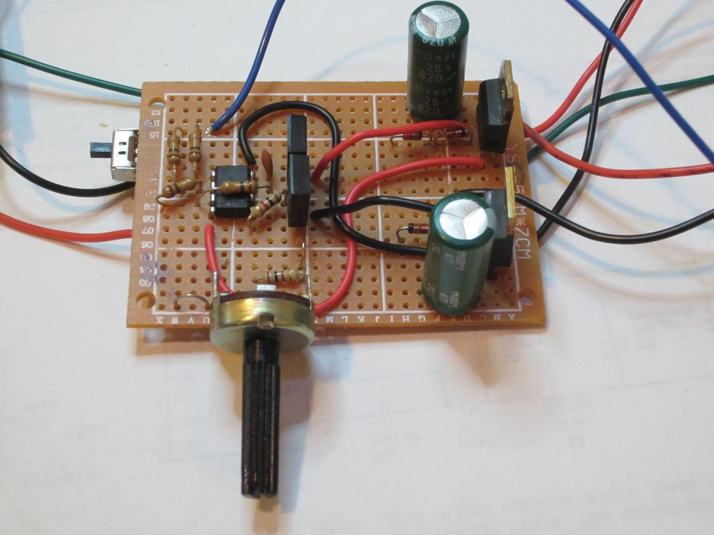
The picture below shows the triangular waveform generator board. The blue trim-pot takes place of R16 (please refer to schematics in my previous post), it is used to fine-tune the output triangular waveform’s frequency and amplitude. The two green trim-pots correspond to R20 and R21 and they are used to set the triangular waveform’s DC offset. For NPN transistors (or N-type semiconductors in general), we want to shift the triangular waveform above 0V. And similarly, for PNP transistors (or P-type semiconductors in general), the output sweep signal should be trimmed to remain negative.
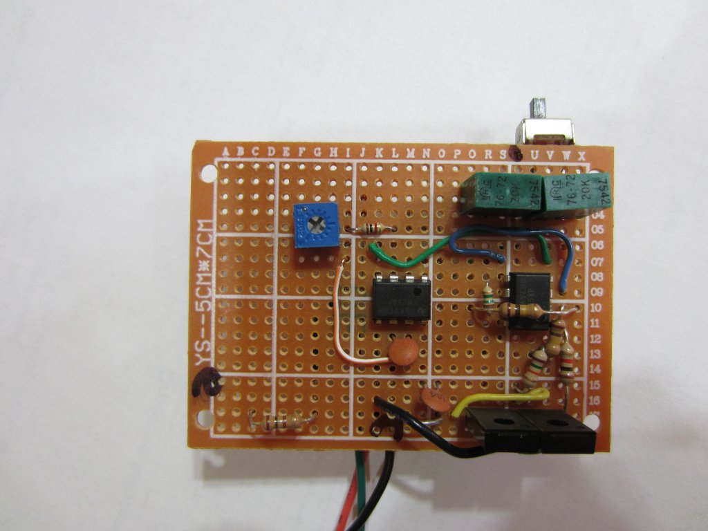
Here is a picture of the staircase waveform generator. A local 78L05 regulator is used to power the logic ICs. The resistors used in the R-2R ladder were hand matched to be within 0.5% of accuracy. Proper wiring and power supply by-passing are absolutely critical when using a protoboard. The best way to make sure everything works correctly is to use an oscilloscope to observe the output waveform at each of the binary counter’s output pin. And if you observe an irregular count (e.g. not /2 /4 /8 /16…), you could almost always be certain that it was due to a signal integrity issue caused by either the board layout or inadequate by-passing.
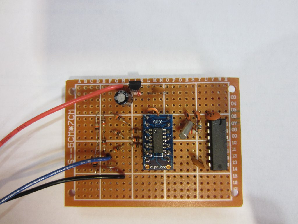
I used yet another board to amplify and shift the base staircase waveform. Also I used two regulators to provide the ±12V needed by the OpAmps. To switch between N-type and P-type devices, I used two SPDT switches, one on the triangular waveform generator board and the other on the staircase amplifier board. Of course, ideally you should replace them with a DPDT switch instead.
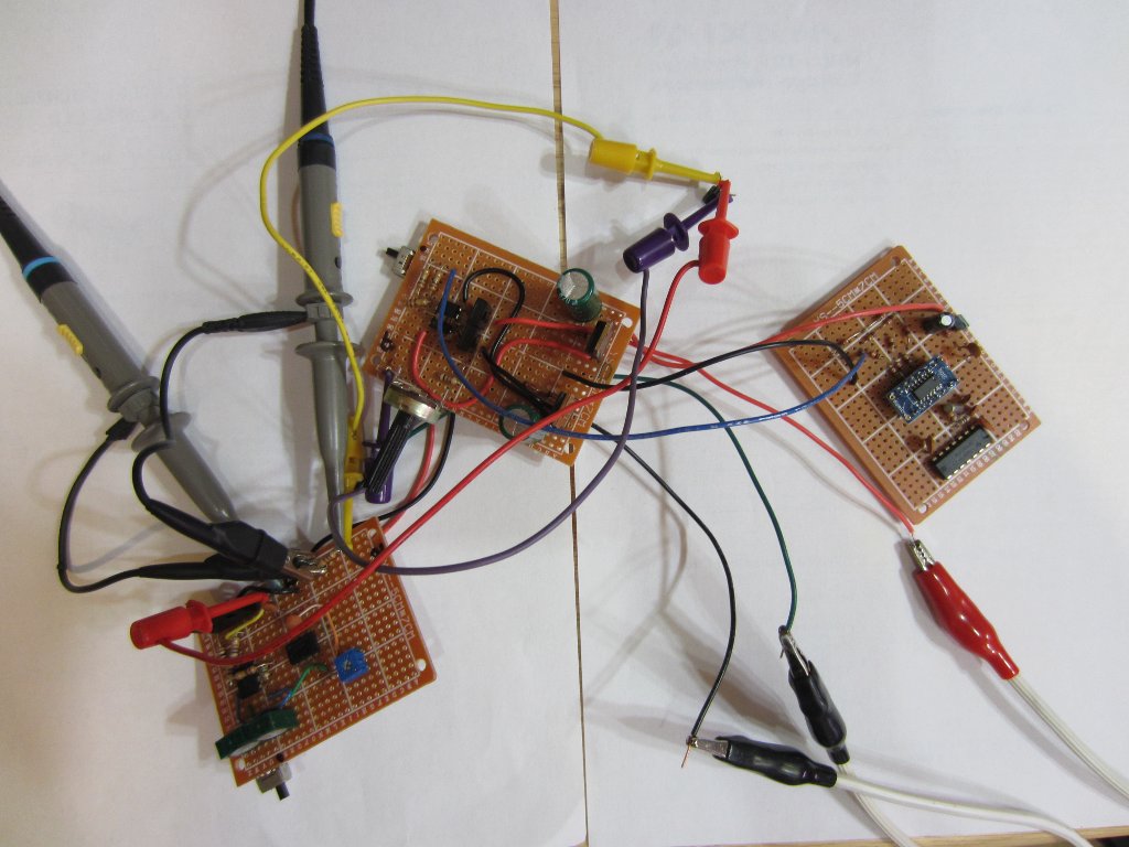
The following picture shows what the test circuit looks like after putting everything together. Power is delivered from the bottom right via a bench power supply, and the DUT (a 2N3904 in this case) is shown in the upper middle section with three mini-grabber clips attached.
Using this setup, I captured the characteristic curves of several devices as shown in the pictures below. The “ripples” in the pictures unfortunately are the artifacts introduced from the noise picked up by the lengthy wiring. And they are somewhat compounded by the fact that the curve tracer’s ground is different from the oscilloscope’s ground (see schematics in my last post). The purpose of this arrangement was to simply the circuit design as discussed earlier. These artifacts are not as prominent as shown in these pictures in the real world as they are not in-sync with the trigger signal. Because they are unsynchronized, they tend to shift rapidly and become faint background noise. Of course, this noise can be greatly suppressed with a properly designed PCB and shortened wiring.
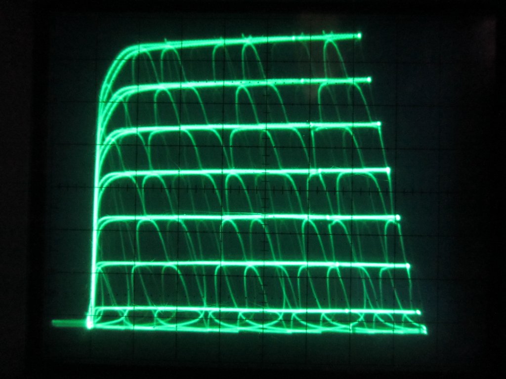
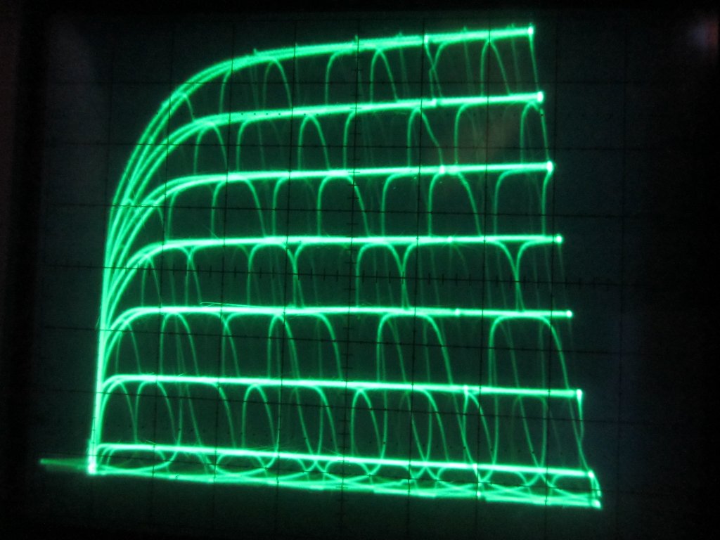
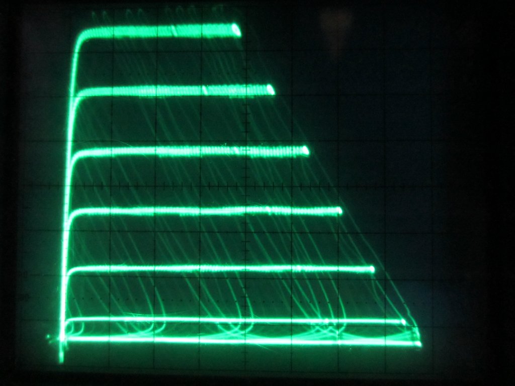
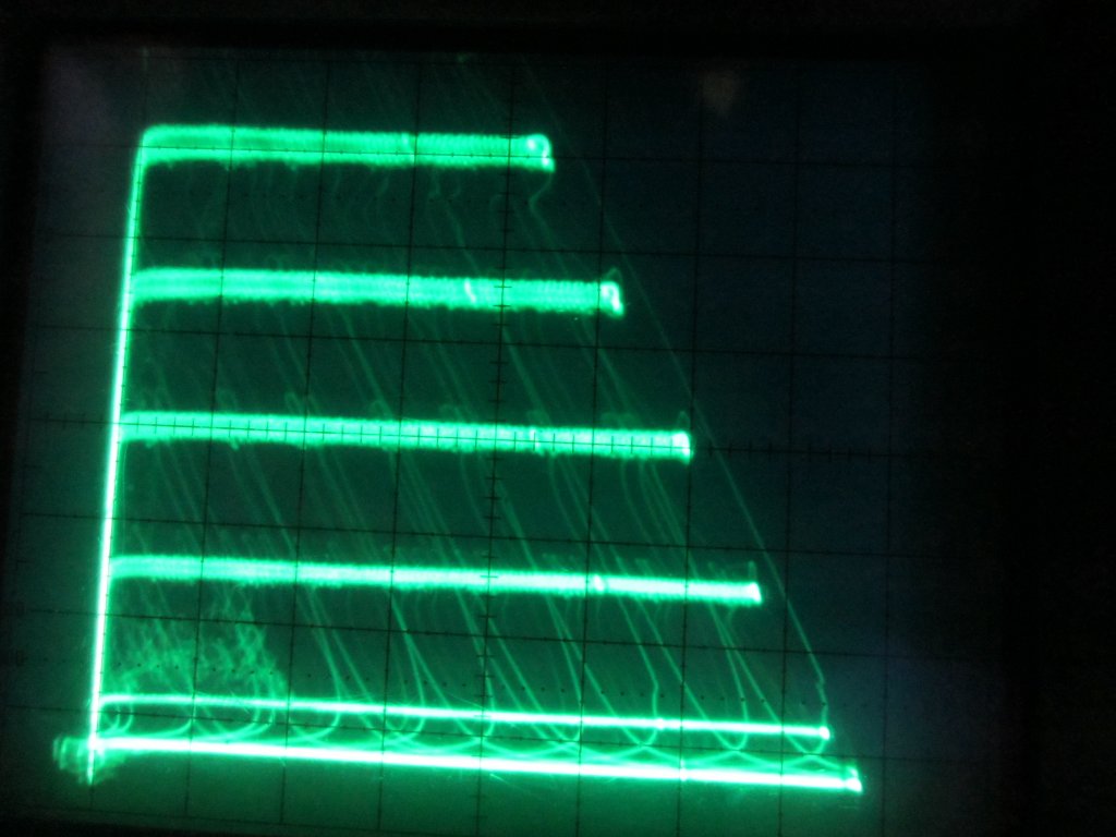
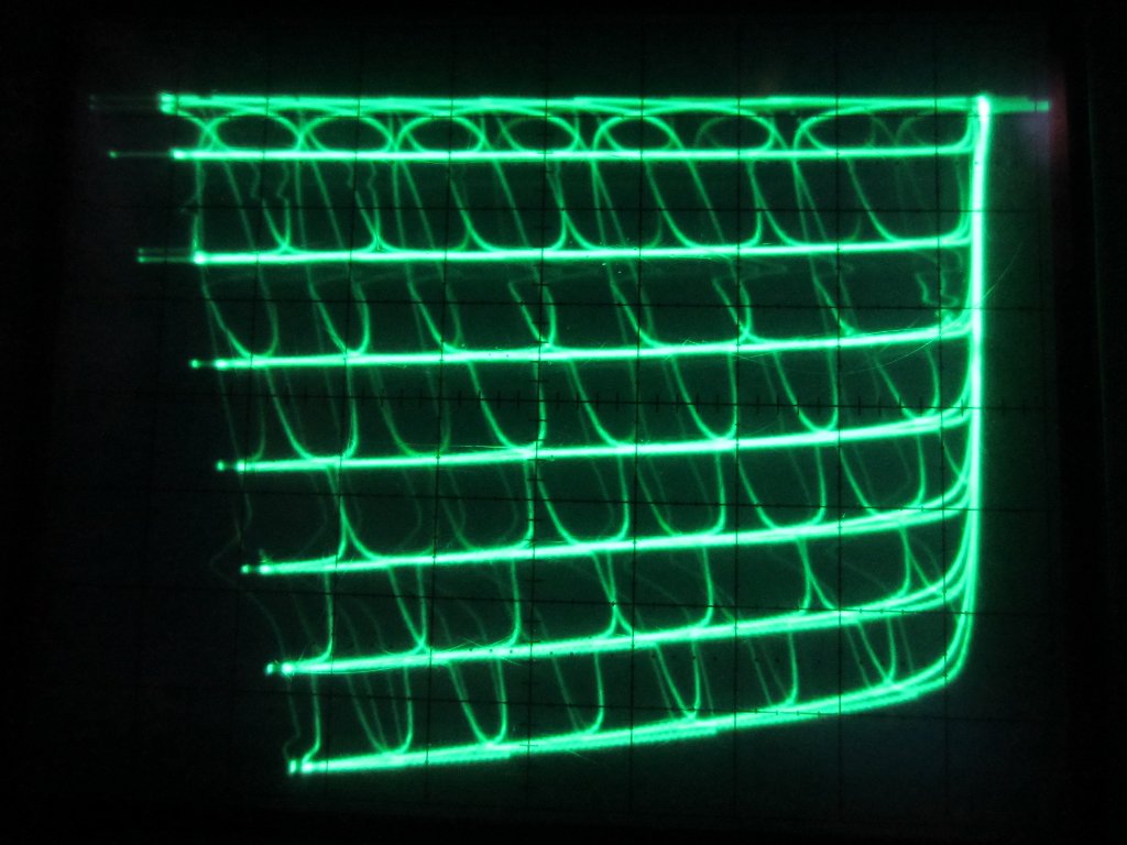
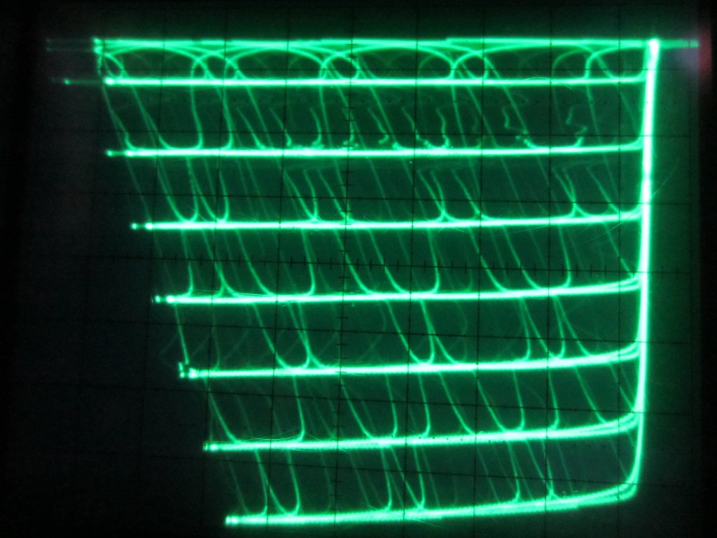
The first two pictures below are the characteristic curves of two small signal NPN transistors. The one on the left is a general purpose 2N3904 and the one on the right is a high frequency NPN epitaxial silicon transistor SS9018. In both cases, the base resistor was set to the max value and the base current is roughly set at 80 uA per step.
 |
 |
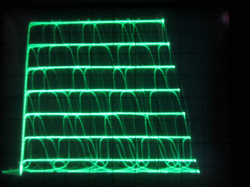
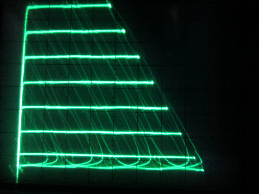
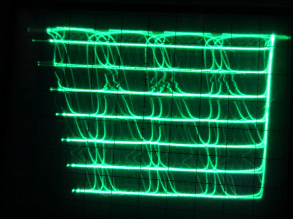
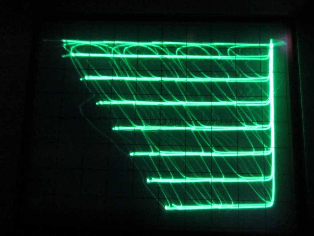
The next two pictures are the characteristic curves of a medium powered NPN transistor (BD137) and a high power NPN transistor (TIP35C). The base current was adjusted to roughly 0.5mA per step for BD137 and 2mA per step for TIP35C.
 |
 |
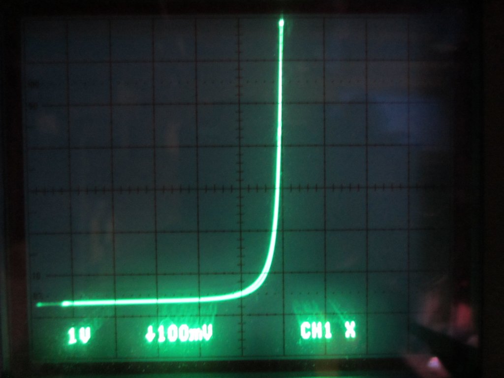
The curve tracer can also be used to trace MOSFETs’ characteristic curves. Since MOSFETs’ gates do not draw any current in steady states, the Vgs steps are fixed regardless of the value of R28 in this setup. Of course, you could add a voltage divider on the “b” output to change the gate voltage if it is desired. One thing to pay attention to is that while the gates of MOSFETs are insulated, due to the inherent gate capacitance it takes time for Vgs to change. When the gate is driven from a high resistance source, this rise/fall time can become more pronounced. So, in order to obtain a “clean” trace for MOSFETs, you will want to turn R28 all the way down. If you increase the gate resistor (R28) you will see that each characteristic curve diverges from the end, depending on whether the sweep triangular waveform is rising or falling. In the pictures below, the gate potentiometer was turned all the way down, but you can still see the aforementioned gate capacitance effect manifested as widened traces. This phenomenon is more pronounced for power MOSFETs (such as BUZ101S on the right) than on small signal MOSFETS (such as 2N7000 on the left) due to the larger gate capacitance.
 |
 |
Using this curve tracer, it is also possible to trace the characteristic curves of other semiconductors. Here are a couple of examples: the first picture shows the characteristic curve of a 5V Zener diode (the base signal is left unconnected) and the second picture shows the characteristic curve of a TRIAC (BTA10-660, gate is connected to the staircase signal) with different Ig’s.
 |
 |
To measure P-type devices, all we need to do is to flip the polarity switch. Here are the characteristic curves of a couple of general purpose small signal PNP transistors (2N3906 and 2N4403)
 |
 |
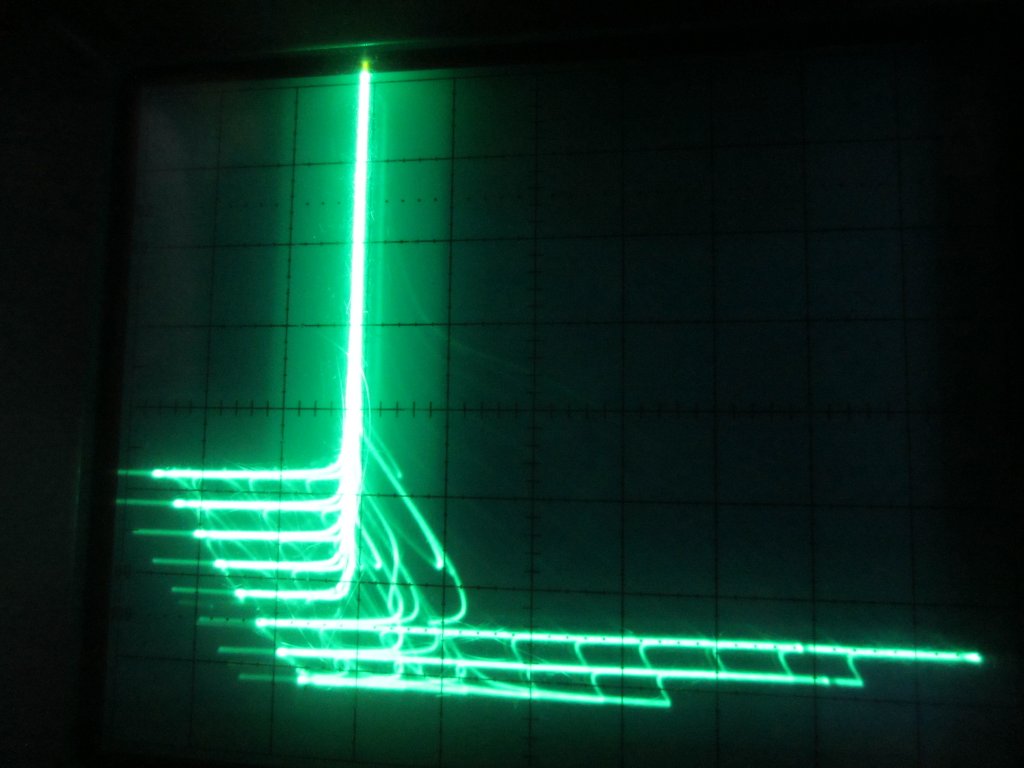
And the last two pictures are for a medium power PNP transistor (BD138) and a high power PNP transistor (TIP36C). The base current settings are similar to those of their NPN counterparts.
 |
 |
Note that in all of the above pictures, channel 2 (y channel) is inverted, if your oscilloscope doesn’t support inverted channels the images you see will simply be mirrored horizontally.

