Power supply is one of those things one can never have too many of. I have quite a few already, and my favorite one so far is the Topward 6603A. This dual 60V/3A tracking power supply satisfies most of my needs. I have since added an automatic fan controller, digital voltage readout and a fine voltage adjust knob, making it even more pleasant to use. Another power supply that I regularly use was the one I built earlier last year. That power supply was based on an LM338 5A voltage regulator with added digital voltage/current readouts. But I have always wanted to build a power supply more or less from scratch without using those three terminal regulators. So this time around, I decided to design and build one from the ground up.
In a recent local auction, I bought two huge aluminum heatsinks. I used one in my electronic load project and I have another one left over. I thought it would be perfect to use the other heatsink to build a beefy power supply given its heat dissipation capability, although it probably is an overkill. I also have an old Deltron W127G open-frame power supply lying around. The W127G is rated for 24V 10A output, but the transformer it comes with is rated at 540W (W127G used a full-wave rectifier instead of a bridge rectifier). The secondary winding is center-tapped and produces roughly 2x28V AC. So my plan was to design a power supply that uses the transformer in the W127G and at the same time leverage the big heatsink I got.
Here are some of the design goals I had in mind given the power transformer and heatsink I have:
- Voltage adjustable from 0 to ±30V
- Current limit adjustable from 0 to 10A
- Precision voltage tracking
- Digital voltage/current control
And here are some of my preliminary designs in LTSpice:
You can download the SPICE models I created here: DualTrackingPowerSupply.tar.gz
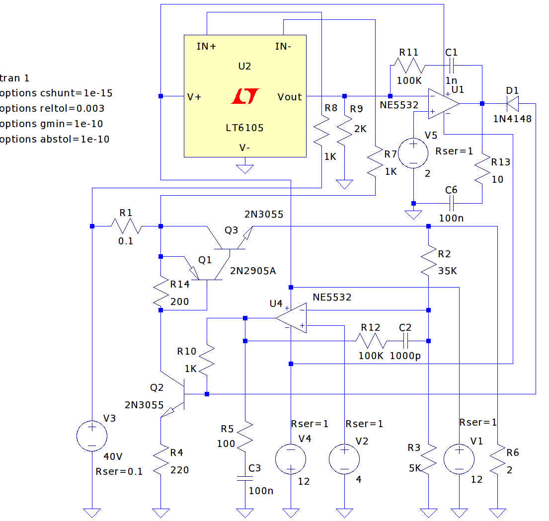
First, let us take a look at how the positive side works in constant voltage and constant current mode:
The voltage after rectification and filtering comes in at roughly 40V, this is illustrated by voltage source V3. The current flows into Q1 and Q3 via shunt resistor R1. The voltage drop across R1 is used to set the current limit, which I will explain later on. Voltage source V2 is connected to the positive input of the OpAmp U4. The output of the OpAmp is adjusted via the feedback loop (via R10, Q1, Q2 and Q3) untill the voltage at the negative input equals that at the positive input. When the system is in equilibrium, the output voltage equals:
\[V_o=\frac{R_2 + R_3}{R_3}\times V4\]
Thus, by adjusting the reference voltage V2, the output voltage can be adjusted continuously. In the parameters illustrated above, the voltage adjustment is between 0V to 32V when V2 varies between 0V and 4V. The choice of the reference voltage V2 is not arbitrary. The control voltage is chosen to be between 0V and 4V because most internally referenced DAC can output up to either 2.048V or 4.096V.
The OpAmp I decided to use is NE5532, it has much higher unit gain bandwidth (10MHz) than other general purpose OpAmps (e.g. LM324/LM358/uA741) and also has much lower noise. These all translate into better regulation characteristics. But we need to be more careful when using a fast OpAmp, as unwanted oscillations could become problematic if not designed correctly. If you are interested in loop stability and phase margin, please take a look at this application note from TI. For this design, a filter network formed by R12, C2, R5 and C3 is introduced to improve the loop stability and prevent this unwanted oscillation.
Another thing I should mention here is the use of Q2. Because the power supply range of NE5532 is less than our ±40 V supply rail, the output swing of the OpAmp is limited by its own power supplies (in this case it’s ±12 V). Since NE5532 is not a rail-to-rail OpAmp, its output swing is roughly ±10 V. In this case and Q2 is needed to extend the control voltage range at the base of Q1 to include the positive rail. If the power supply voltage range is within the OpAmp’s supply limit, Q2 can be simply removed and the output from the OpAmp can be used to drive the base of the pass transistors directly.
Q1 and Q3 forms a complementary Darlington pair (aka. Sziklai pair). Here, this complementary pair functions like a high-gain PNP transistor. Depending on the output current requirements, multiple power transistors can be paralleled together in place of Q3.
Precision current setting is achieved via U2 and U1. LT6105 is a current sensing amplifier. It’s gain is set to 2 (R9/R8) and the output from U2 is fed into the negative input of the OpAmp U1. The current setting voltage reference V5 is connected to the positive input of U1, and via the negative feedback the OpAmp adjusts its output so that the voltage at both of its inputs are equal. Because the current sensing OpAmp measures the voltage drop across R1, the current set limit is determined by:
\[I_{set}=\frac{V_5 \times R_9}{R_1\times R_8} = 5\times V_5\]
Unlike voltage setting, we are not setting the current output of the power supply but rather setting the maximum allowed current. So D1 is included here so that the control of U1 kicks in only when the current exceeds the preset limit. When the output current is below the limit, U1 tries to adjust its output higher, but the diode blocks the current flow and thus the output voltage is dictated only by V2. When the current limit is reached, the output of U1 goes lower and D1 starts to conduct and drag down the base voltage of Q2. Thus Q1 and Q3 becomes less conductive. This in turn lowers the output voltage until the output current equals the set current limit. When V5 varies between 0 and 2V, the output current limit can be set between 0 and 10A.
So far I have explained how the positive power supply works. Now let’s take a look at the negative side and the tracking mechanism.
Ideally, the negative side should be implemented exactly the same way as the positive side using an independent transformer winding. The two identical channels can then be chained together when used in bi-polar operation. Most modern multi-channel lab power supply designs follow the aforementioned approach. Since the transformer I have is center-tapped, the ground is shared between the positive side and the negative side so I have to implement a true negative power supply using complementary components.
The negative side of the circuit is shown below:
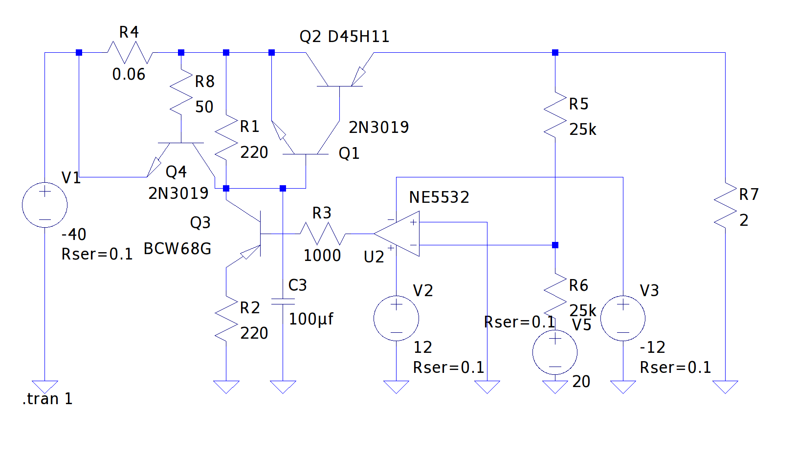
Since LT6105’s differential inputs voltage can not go much below the ground, I could not use it here for the negative side current sensing. In fact, not many current sensing OpAmps have this capability as most high-side current sensing are strictly for positive supply voltage only. So I decided to omit the current setting for the negative portion and add in a fixed current limiter at roughly 10 A instead. The good news is that when the power supply is used in series mode, the current limit can still be set via the positive side.
Here Q4, R8 and R1 forms the current limiter. Q4 begins to conduct when the voltage drop across the shunt resistor R4 approaches roughly 0.6V. Once Q4 begins conducting, the base of Q1 and Q2 is pulled down and thus limits the current flowing through.
Tracking is accomplished via R5, R6 and U2. R5 and R6 are connected in series between the positive output and the negative output terminals. Since R5 and R6 are equal in value, When the positive voltage and the negative voltage are equal the voltage at the voltage divider is 0 with respect to the ground. The voltage divider is connected to the negative input of OpAmp U2. Since the positive input to the OpAmp is tied to the ground, the OpAmp will adjust its output through negative feedback until its negative input voltage equals 0 as well. When the negative input equals 0, the negative voltage will be the same as the positive voltage. This tracking mechanism can be made extremely accurate. Since R2 and R3 are the same value, they can be hand picked and matched. The temperature coefficient of these two resistors are not critical as long as they are thermally coupled (e.g. placed together). So even using cheap carbon film resistors we can achieve great tracking accuracy that is almost independent of the temperature.
The remaining circuitry is almost identical to its positive counterpart, except that Q1, Q2 and Q3 are the complementary versions.
As another note, the transistors I used in the schematics above were just some random ones I could find (with reasonable spec) in the LTSpice library. I will be using the ones I have on hand for my build.
Everything looks good so far. My next step is to build this circuit. Right now, I am planning to use an MCU to control the output voltage and current setting. Once I build the circuit, I will include the updated schematics. Stay tuned.

