In this blog post, let us take a look at a Wavetek 859 50 Mhz pulse generator. This pulse generator was made back in the 1980’s and has long been obsolete since. I got this unit next to nothing as it was not working and I was told that multiple boards might have failed. Even though it might not be repairable, we can still learn quite a bit from a teardown. If you just wanted to watch the teardown video instead of reading through the post, you can scroll down to the bottom.
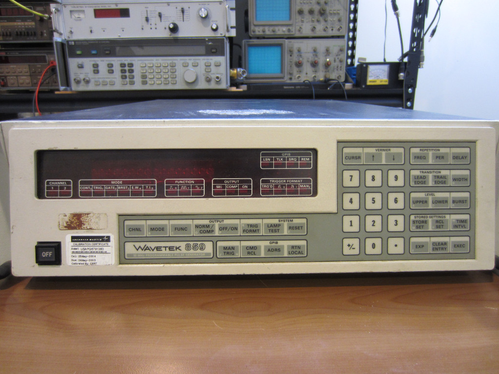
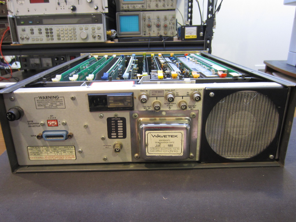
This unit is almost the same size as my HP 8642B synthesized signal generator. The pictures below are the front and the back panels:
|
|
Unlike most of the rack mountable test equipment which offer both front panel inputs and back panel inputs, it appears that Wavetek 859 only came with the rear panel input option. Clearly, it was meant to be mainly used in an automated test environment. The unit I got has option 001 (GPIB) and option 010 (dual channel) installed. As you can see from the picture below, all plugin slots are occupied.
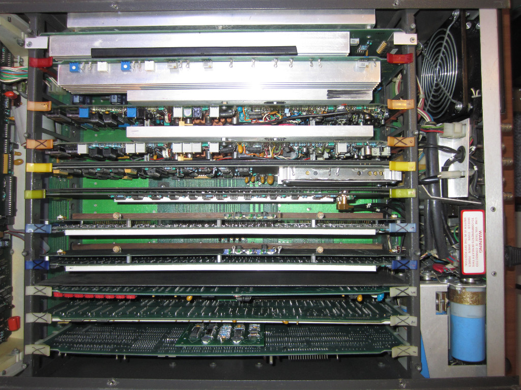
In the teardown below, the cards were removed in sequence from the bottom to top.
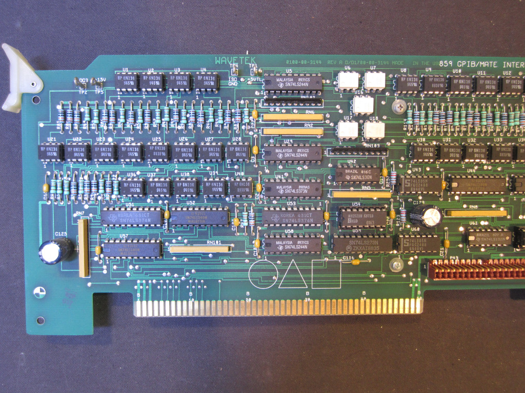
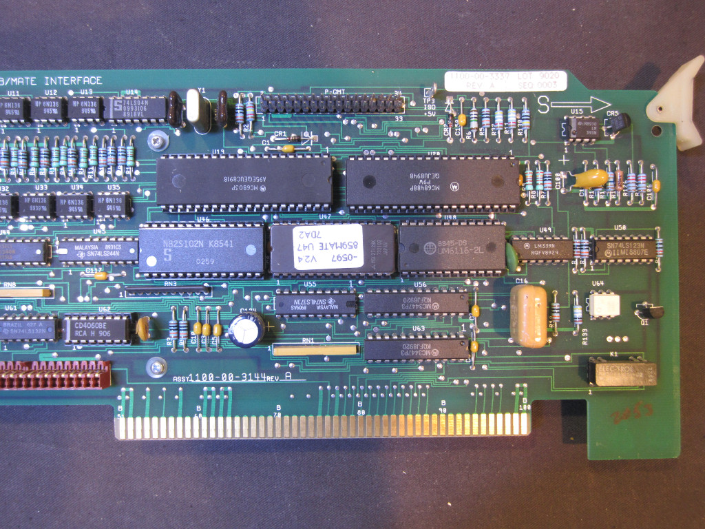
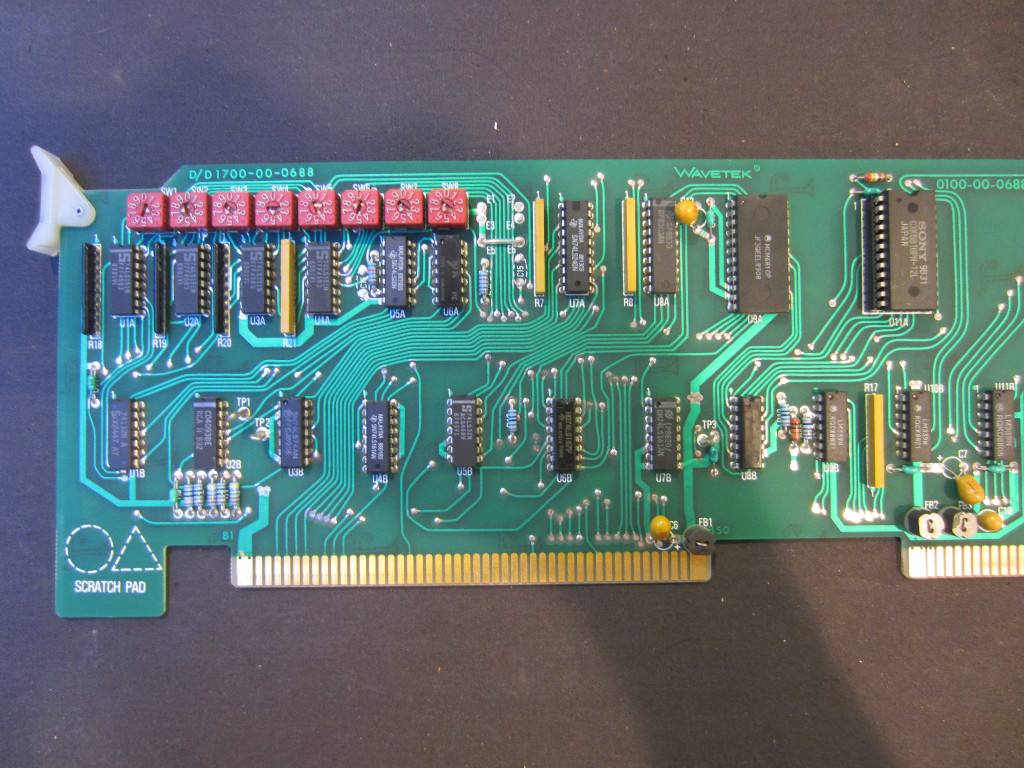
The first set of pictures are for the GPIB interface board (with the optional MATE interface). Compared to many modern single chip solutions, this board certainly looks overcrowded. But it does offer an isolated GPIB interface. The optocouplers used here are 6N136‘s and 4N26‘s. The GPIB IC is a Motorola MC68488P. The silkscreen “S” with an arrow on the board indicate the direction for wave soldering.
|
|
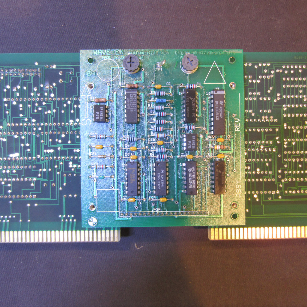
On the other side of the GPIB board, there is a small daughter board. I am not entirely sure what this board does. It has a DAC1006 DAC chip on it. The daughter board is mated onto the main plugin board via headers and secured via standoffs.
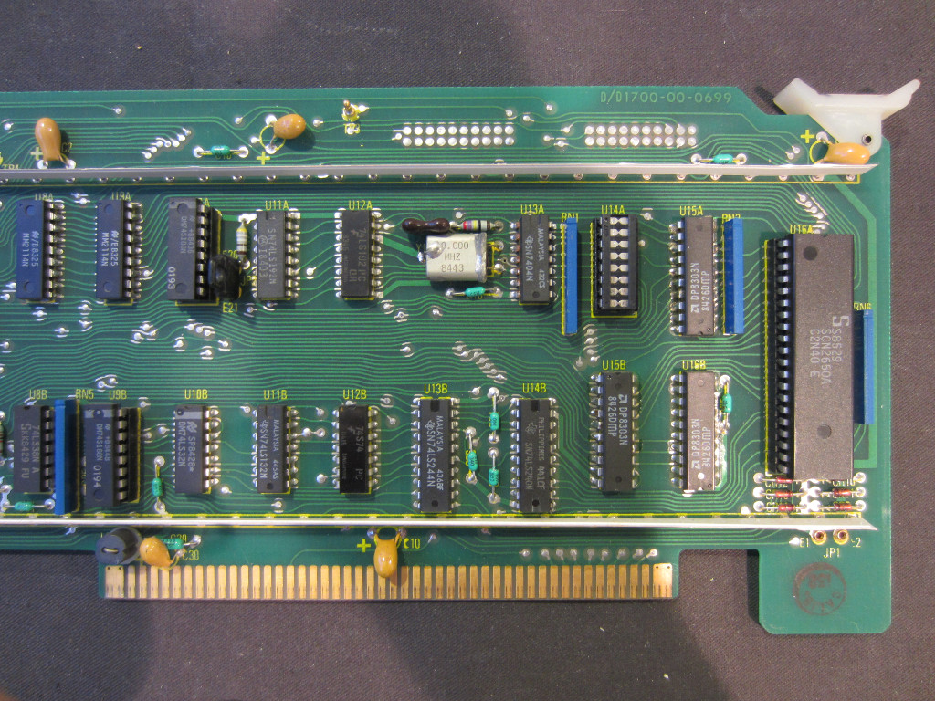
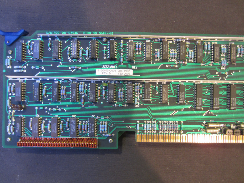
The next board is the main controller board. The microprocessor used here is a Philips SCN2650 (I couldn’t find any information on this chip though). The MCU is clocked at 10 MHz.The firmware is stored on five 16 Kb MM2716 UV erasable ROM. There are two empty sockets, I am not sure if they are intentionally left blank for some optional firmware packages or they are missing. If these two sockets were supposed to be occupied, it would have explained why the unit failed to boot at the first place.
|
|
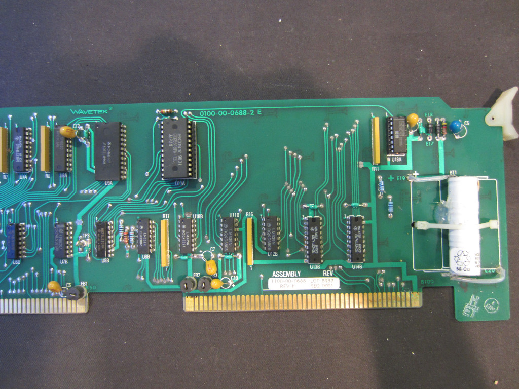
The next board in line is what I believe the circuitry used to store various timing parameters, as it contains a battery backup and a 16 Kb SRAM chip (Sony CXK5818). like many test equipment back then, parameters are stored in battery backed-up SRAM (flash memory had not been invented back then yet).
|
|
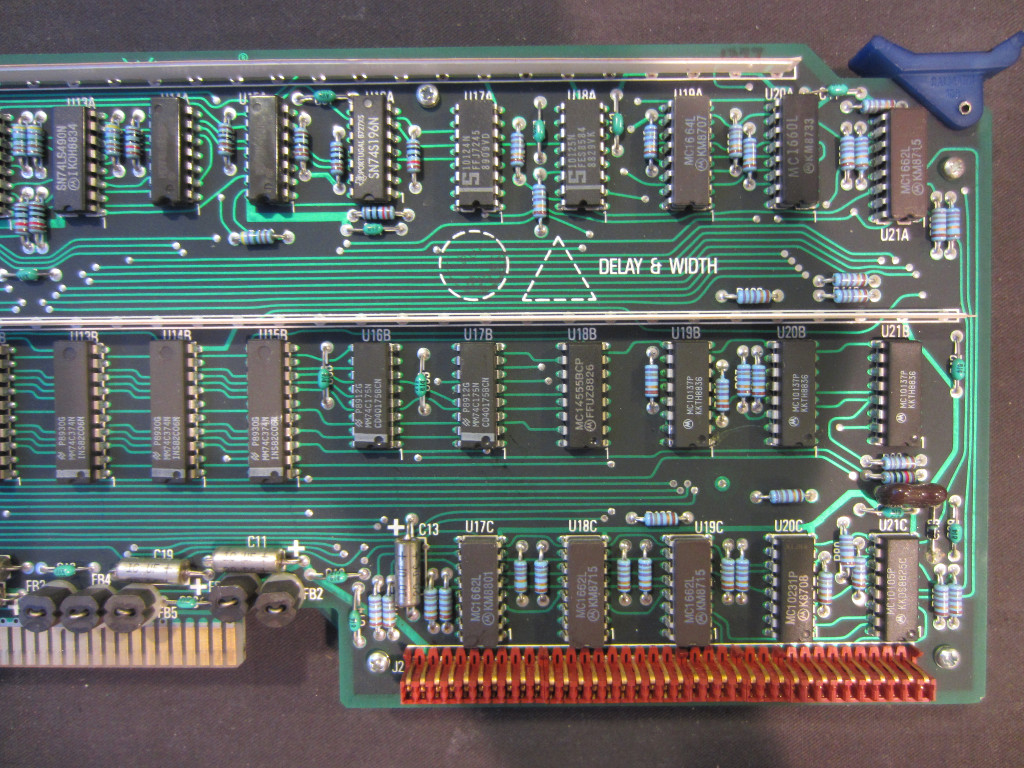
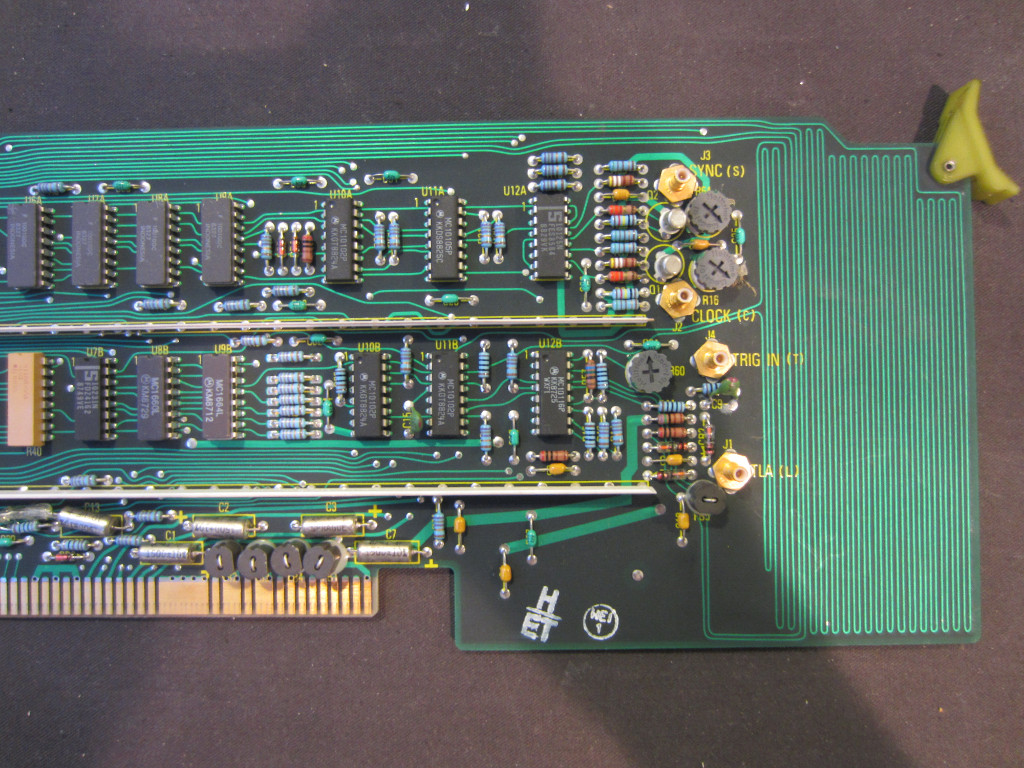
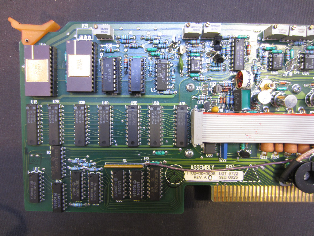
The pictures below are one of the two boards that handle some kind of timing logic (delay and width). I could tell they are channel specific as these two boards are identical, one for each channel. Among the logic chips on this board are some gates (MC1662), flip-flops (MC10231) and counters (MC10137, SN74S196).
|
|
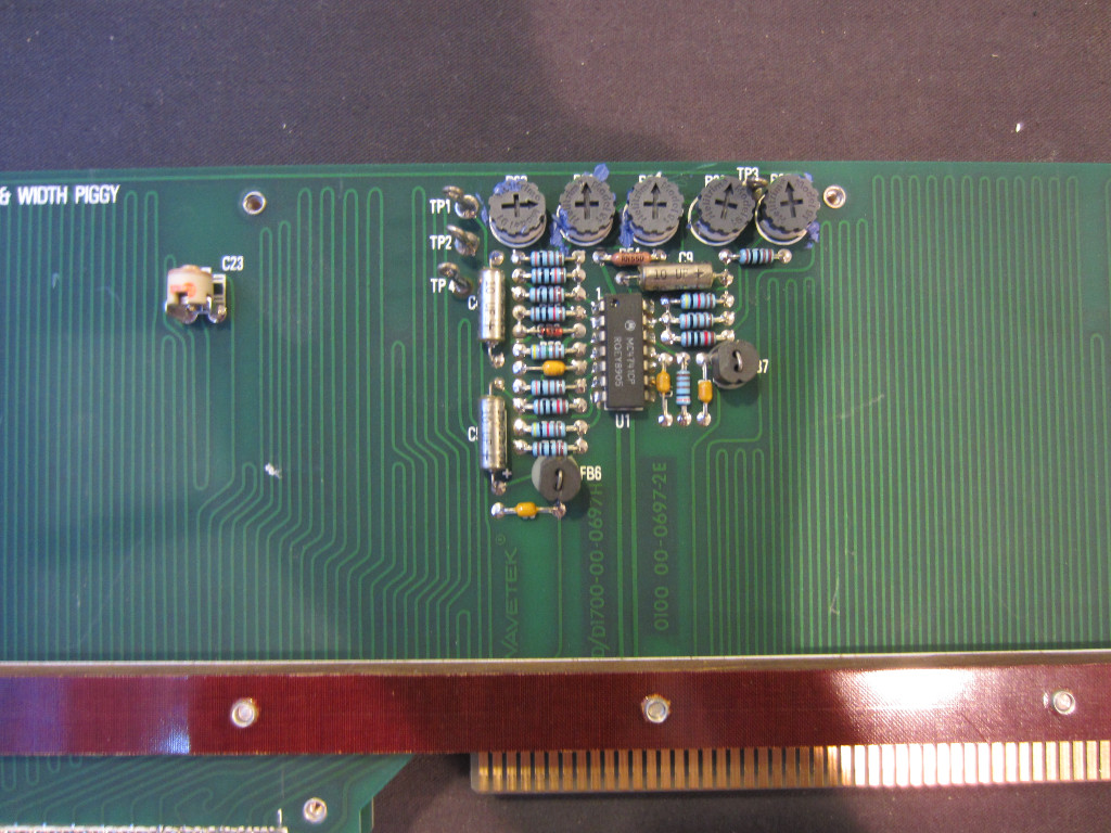
Piggybacked on a separate PCB plugged into the one shown above is the delay logic board (the silkscreen says Delay & Width Piggy). The delay lines are implemented via on-PCB etched traces. In fact, most real estate on this PCB is dedicated to those delay lines. The chip in the center is a quad 741 OpAmp. This board plugs into the board above via headers (you can see the brown female headers in the pictures above), and to increase rigidity, a thick bar is mounted across the PCB.
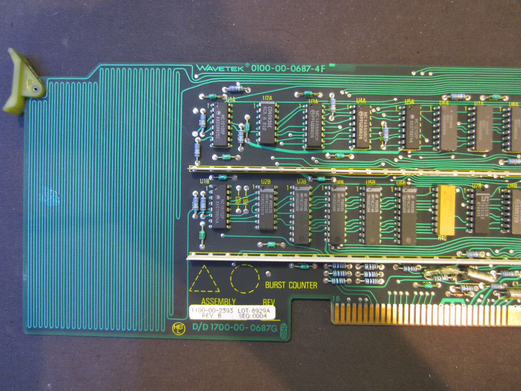
The next board is the burst counter assembly. Again, delay lines were directly etched onto the board. Signals are brought in from, and out to the rear panel BNC connectors via those four coaxial connectors.
|
|
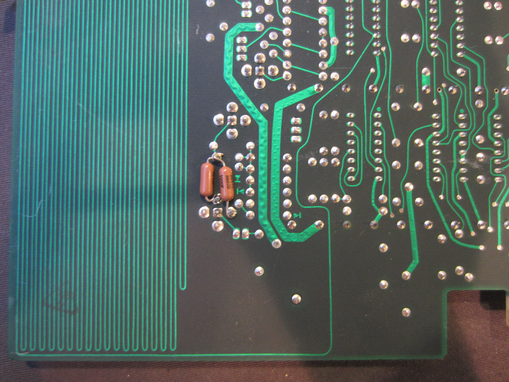
A couple of bodges can be seen on the back side of the board.
| [adsense] |
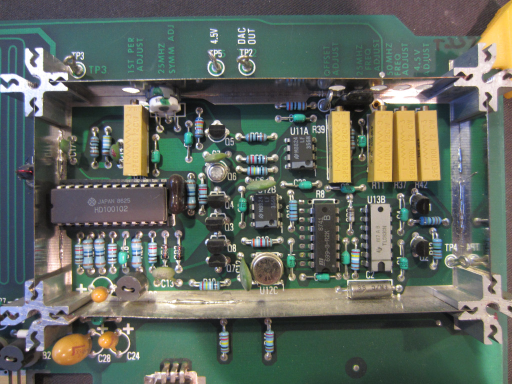
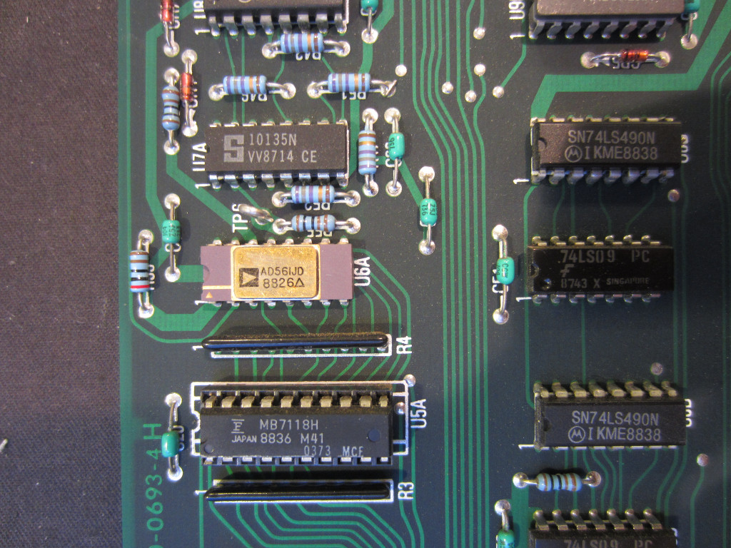
The next board is labeled as Clock OSC. It is used to generate the 25 MHz and 50 MHz reference signals. Again, you can see some delay line structures etched on the board. The DAC used on this board is an Analog Devices’ AD561JD 10 bit monolithic DAC which utlizes a buried Zener high stability voltage reference. Although quite old, this DAC is still available today at more than $50 a pop.
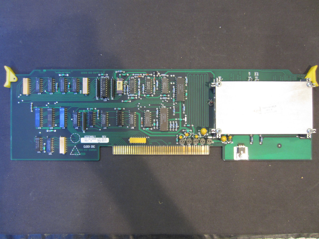
Part of the circuity (the analog portion) is shielded. The shielding is needed to reduce coupled noise. In the picture below to the right, you can see a closeup picture of the AD561JD.
|
|
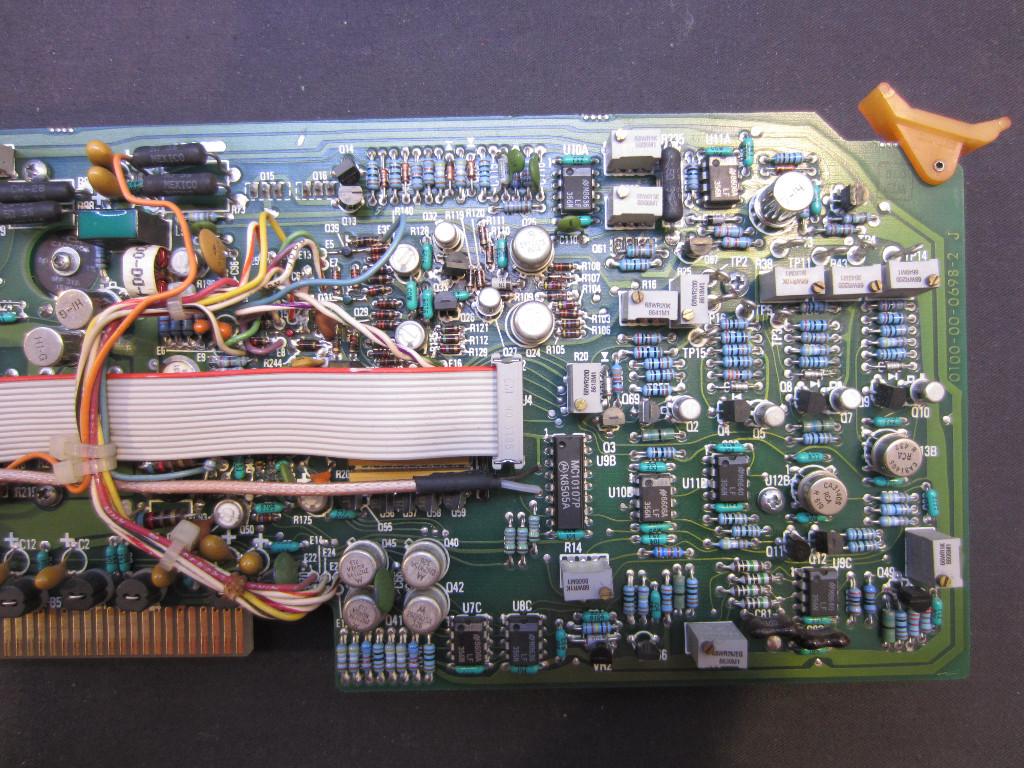
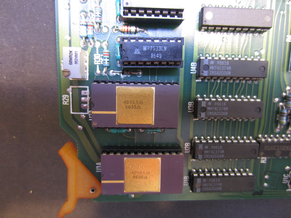
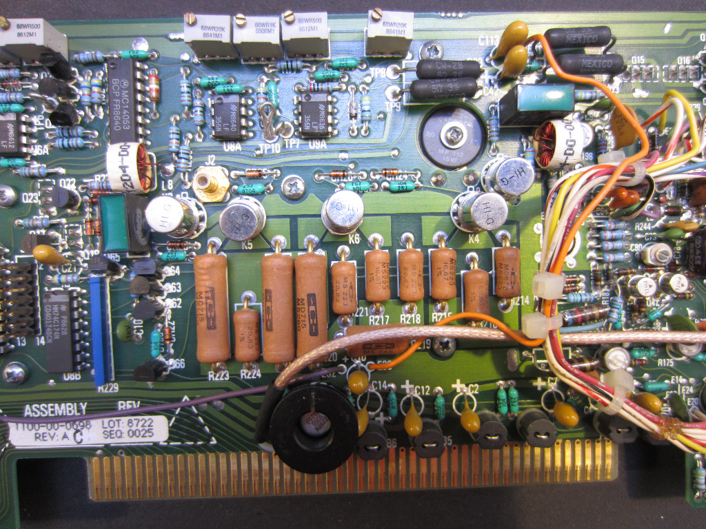
The next two identical boards (one is shown below) are responsible for each channel’s output stage. They certainly look more complex than the other boards we have seen so far. There are a lot of OpAmps (CA3140, LF356) and many precision resistors on this board.
|
|
The two ceramic chips are AD565JD, Analog Devices’ high speed 12 bit DAC. Like AD561JD, these chips also feature the buried Zener for improved stability. And as you can imagine, they are also very pricey. The two channel configuration uses four such chips, two per channel. Now I started to wonder how much this pulse generator cost back in its prime days. Given the large number of ceramic chips and fast high precision DACs, I bet that it would have cost a fortune.
|
|
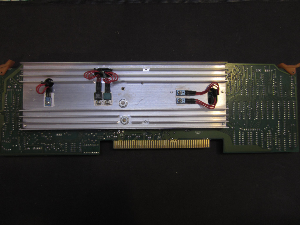
The power transistors responsible for driving the output are mounted on a massive heat sink on the back of the board.
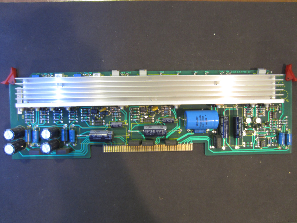
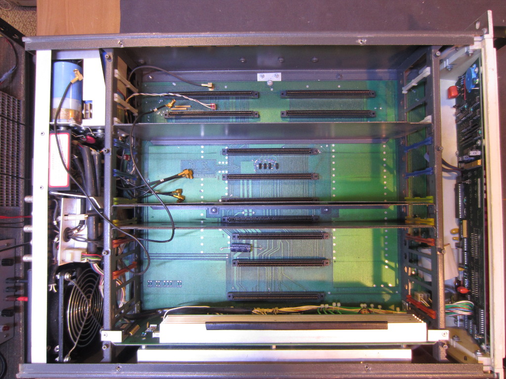
The next board is the power regulation board. Because Wavetek 859’s output channels are isolated, two sets of independent power rails (±15V and +35V) along with a few auxiliary rails are generated via linear regulators. There is another power supply/distribution board (you can see it mounted towards the edge of the case in the last picture towards the end). That board supplies power to the front panel and possibly provides some pre-regulation and protection.
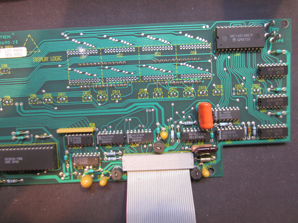
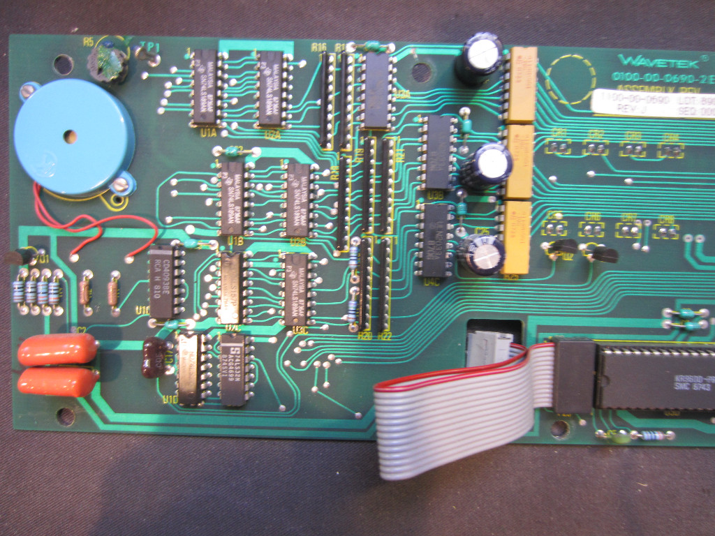
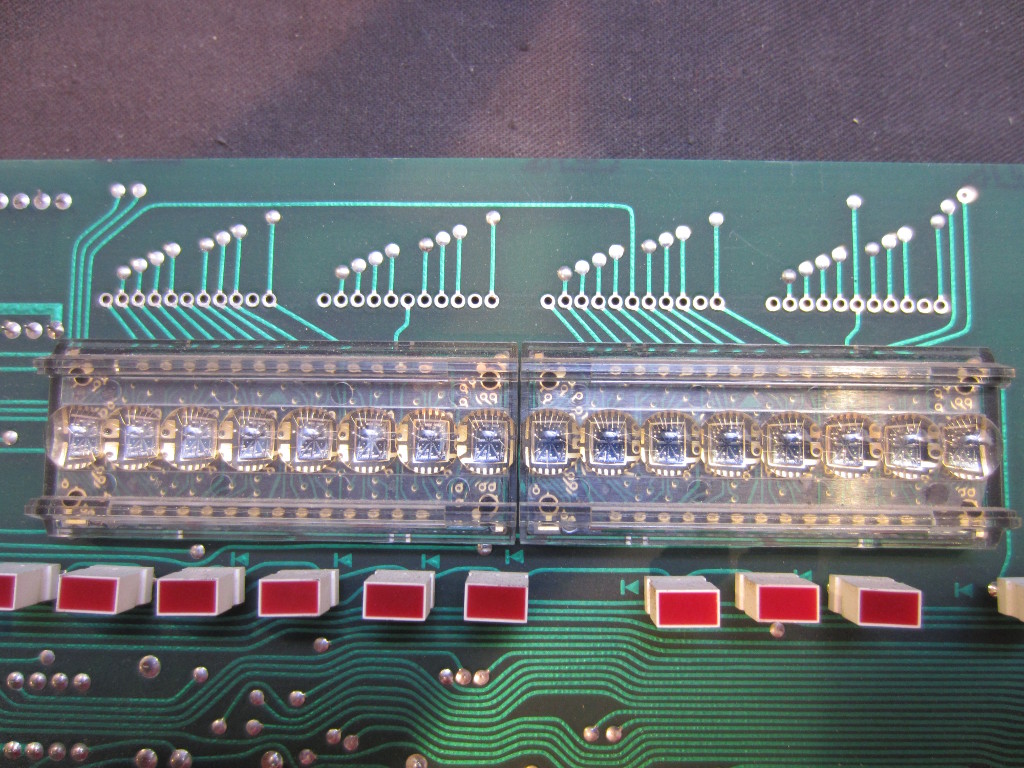
The front panel has its dedicated PCB to handle display and input. The keypad is encoded via KR9600-PRO.
|
|
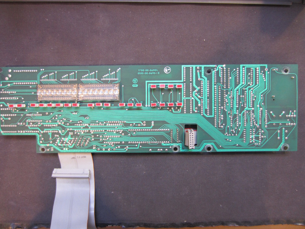
The LEDs and segmented displays are located on the other side of the board facing the front panel.
|
|
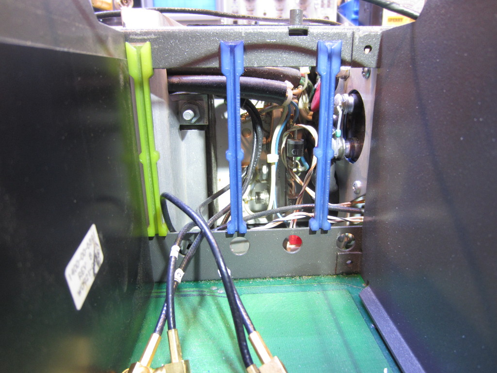
Here is a picture showing the board mounting rail guide, you can see a few power diodes and large capacitors mounted behind near the power transformer. The picture to the right shows the main board with everything removed.
|
|
Finally, here is a video of the teardown.
|
View on YouTube in a new window |
Update
I just repaired this pulse generator, please see my latest blog posting here.

