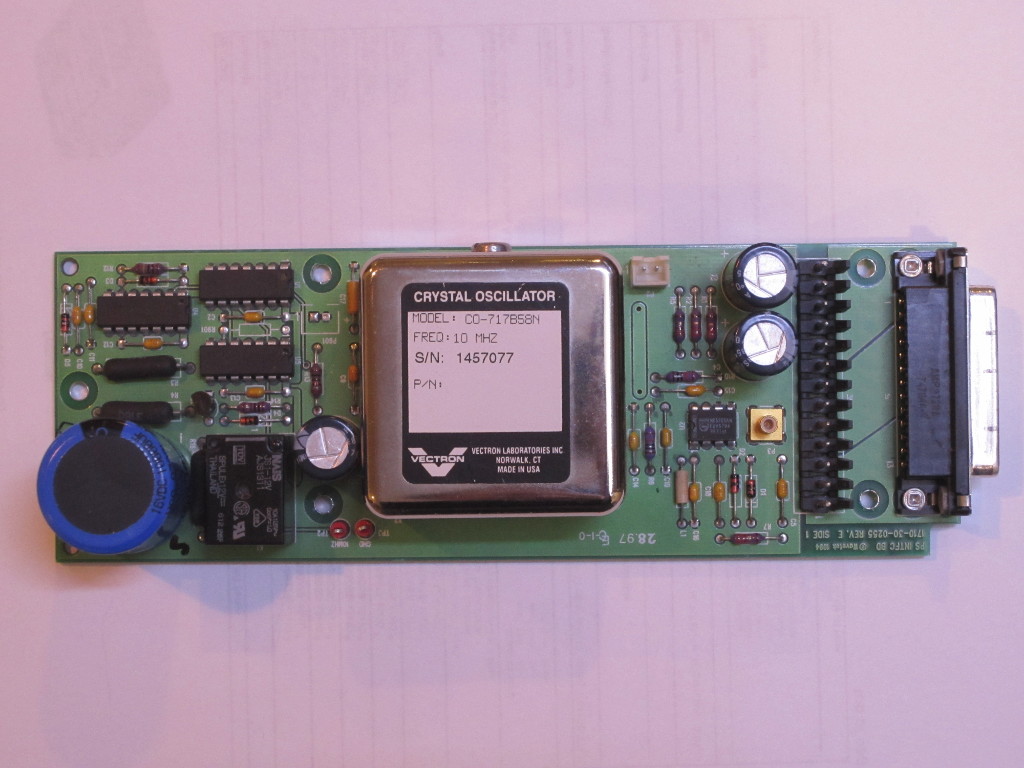
I bought a Wavetek OCXO board a long while ago. My original plan was to remove the onboard crystal oven to replace the broken OCXO in my HP 5350B. But since I later managed to fix the original OCXO , this board had been sitting quietly in one of my component bins collecting dust.
Since I don’t desperately need the crystal oven oscillator any more, I decided to dig a bit deeper to see how this board works and what it was originally designed for.
Unfortunately, the only identifiable information on the board is the marking on the corner:
PS INTFC BD ©Wavetek 1994
1710-30-0255 REV. E
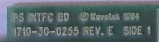
Clearly, it is some kind of interface board as the marking suggested. But after combing through the Internet, I could not find any service manuals or schematics for this board. So I am not quite sure what Wavetek equipment this board was originally designed for.
The OCXO used on this board is a Vectron CO-717B58N, which has a temperature stability of ±5×10⁻⁸ between 0°C to 50°C. The temperature stability of this particular OCXO is actually not that great. In comparison, the temperature stability of the OCXO’s used in most of my HP test gear is at least twenty times better over the same temperature range.
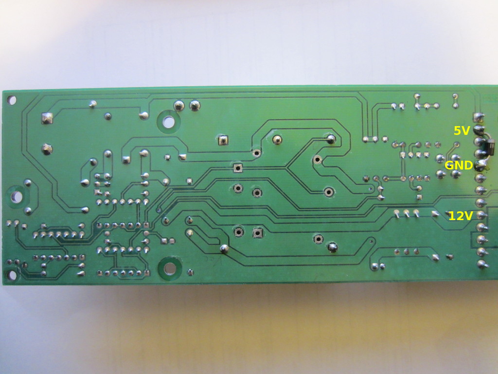
Reverse engineering a two layered board like this one is not very difficult. My favorite method is to take a picture of both the top side and the bottom side of the PCB and use some photo editing software to flip the bottom side of the PCB image so that the traces look as if they were seen through the top layer. Using this method, we can quickly identify the connections among the various components and traces.
Of course, depending on the complexity of the circuits and the components layout, it remains a painstaking process.
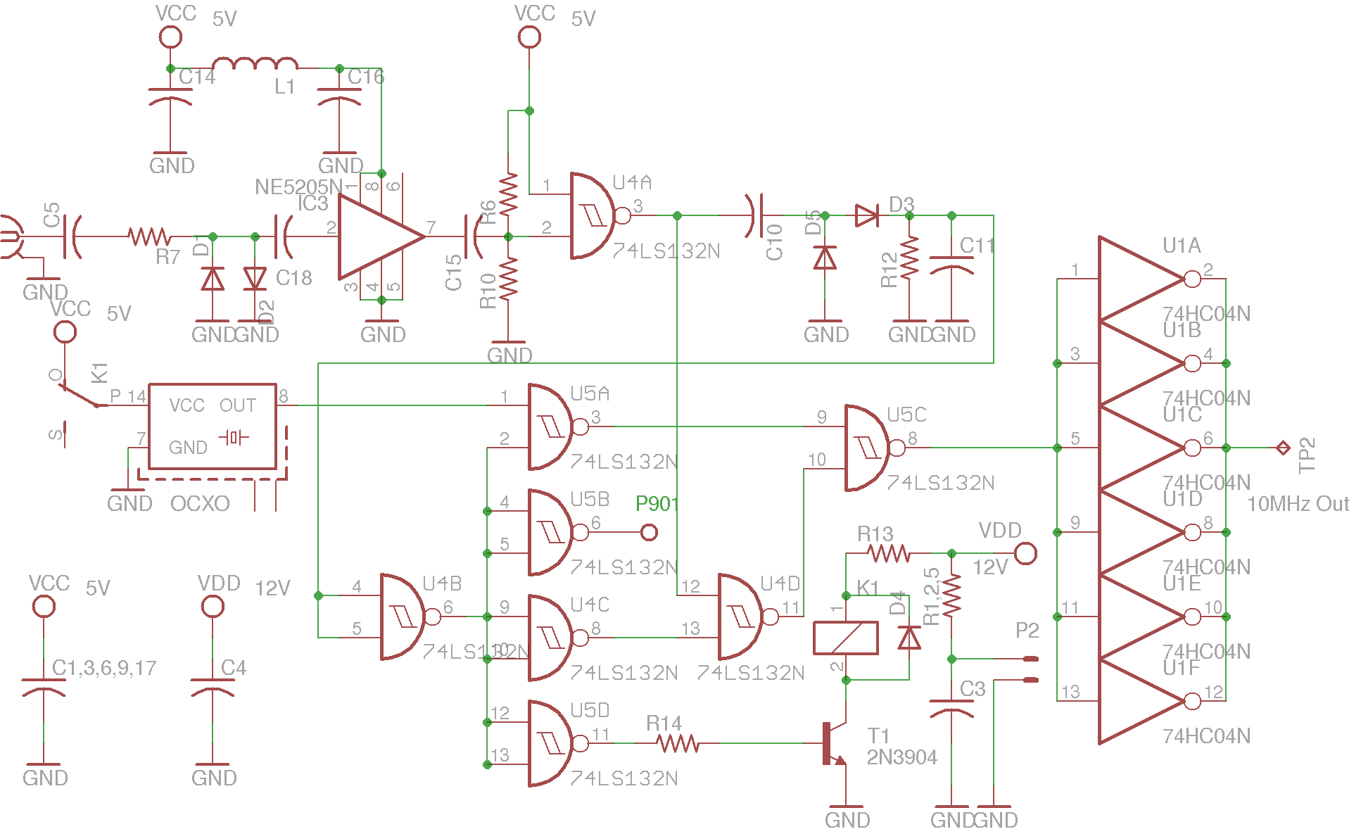
The following are the reverse engineered board pinout and circuit diagram (a couple filter capacitors are ignored in the schematics). Note the diode added between the +5V rail and the ground, I added it for reverse polarity protection.
(click for high resolution images)
Principles of Operation
This board services as a precision timebase. Its output frequency can come either from the onboard OCXO or an external source.
Upon applying power (+5V), the crystal oven begins warming up and achieves its operating temperature within ten to fifteen minutes. The Vectron OCXO used here (CO-717B58N) does not have an oven ready pin and will output the 10MHz signal as soon as power is applied. The 10MHz signal goes through a few 74HC132 NAND gates with Schmitt-trigger inputs and then output via the 74HC04 buffer. The six inverters inside the 74HC04 are paralleled together to increase the output driving ability.
The OCXO only needs a single 5V to operate as the relay connecting the OCXO positive supply input to the 5V is normally closed. When no external signal is present at the MCX input or the 12V supply is not applied, the output from D3/D5 detector is low and thus the input into U4B is also low. Because the two inputs of U4B are connected, U4B serves as a single inverting Schmitt-trigger. Thus, the output from U4B, which is the input of U4C will be high. U4C inverts the signal and outputs a low. The output from U4C enters U4D. Because one input into the NAND (U4D) is low, U4D will outputs a high regardless of the other input coming from U4A (though U4A’s input is biased such that it will output a low when there’s no signal at the input). So the output from U5C is the complement of its input from pin 9. Because the output from U4B is high as mentioned earlier, the output from U5A is only dependent on the input signal from the OCXO. So the OCXO output first gets shaped by U5A and then inverted by U5C. Finally the signal is buffered by the paralleled 74HC04 (U1) and output to the test point and the DB25 connector (not shown in schematic). The relay is not energized in this case when there is no external signal input, even if the 12V supply is present. This can be clearly seen as the transistor that’s driving the relay is connected to the output of U5D, which inverts the U4B output. Because the output from U4B is high, the output from U5D will stay low.
So if only the onboard crystal oven is needed, you only need the +5V supply. Now let’s take a look at what happens when an external clock signal is connected to the input MCX connector. NE5205 is a 20 dB gain wideband amplifier. According to its datasheet, it has a saturated output level of 5 dBm at 10 MHz when using a 5V supply. When an external signal is present at the input, the signal gets amplified by NE5205. When the output amplitude is sufficiently large, the detected signal at the cathode of D3 will drive the input to U4B to high. And thus the input to U4C and U5D will be low. The output from U5D will be high and turn on the transistor which engages the relay. This causes the OCXO to disconnect from the 5V rail and thus stops its output. In the mean time, U4C will also output high, thus the output from U4A will be inverted via U4D. Because the OCXO is no longer connected to power, it pulls down one of U5A’s inputs. So U5A will output high and thus the output from U5C will be only dependent on the input at pin 10. And the input to pin 10 is only determined by the output at U4A as we determined earlier so now the output buffer is driven by the external clock source only.
So this circuit presented a convenient way to switch between one signal source and another depending on which one is present. Because the external signal is not phase locked to the OCXO, the flip side of this circuit is that any RF signal of sufficient amplitude could cause the output to switch. But this should not be an issue as I presume that the board was designed to be used with a known frequency source.

