Typically, a lab power supply can only operate within a single quadrant. Take a positive voltage power supply for example, it can only output or source current. If any attempt is made trying to sink current into the power supply by connecting a voltage source with a higher voltage than the output voltage of the power supply, the power supply would lose regulation since it cannot sink any current and thus is unable to bring down and regulate the voltage at its output terminals.
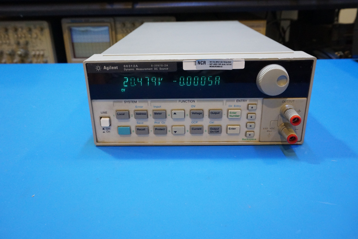
The Agilent 66312A dynamic measurement DC source however is a two-quadrant power supply, it not only can source up to 2A of current between 0 and 20V, but also can sink up to 1.2A or 60% of its rated output current as well. Although lacking some key functionality of a source measure unit (SMU), Agilent 66312A can nevertheless be used in similar situations where both current sourcing and sinking capabilities are needed.
The current sinking capability is accomplished via the so-called down-programmer. Because the down-programmer can sink current, it can act as an electronic load. Conveniently, it can also discharge power supply’s output capacitor and thus improve power supply’s transient response. For instance, 66312A’s transient response time is rated at less than 100µs.
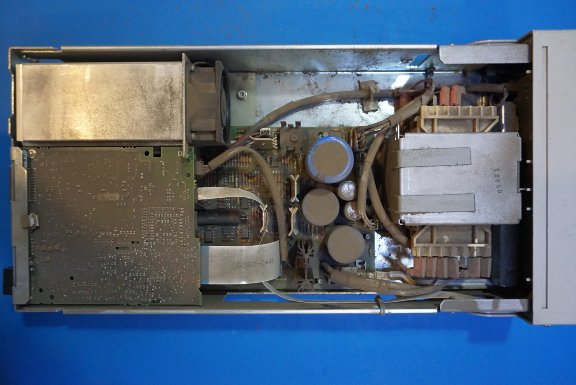
Like most of the test equipment in my lab, this one was also bought on eBay. And this unit was definitely well used in its prior life. These pictures below were taken after I initially opened up the case. As you can see, the entire interior is covered with a thick layer of dust. Presumably, the unit was operated in a dusty environment and was left on most of the time.
|
|
So the first thing I did was taking the boards out of the chassis and gave them a thorough cleaning using 99.9% isopropyl alcohol.
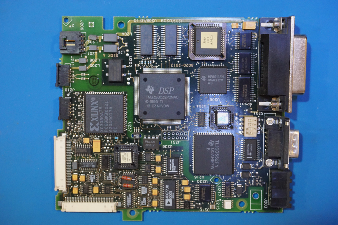
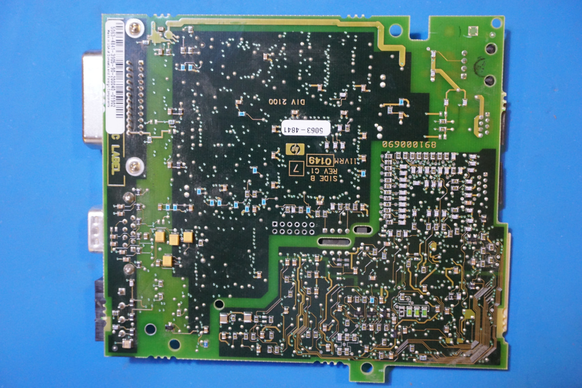
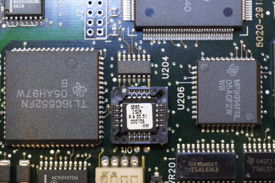
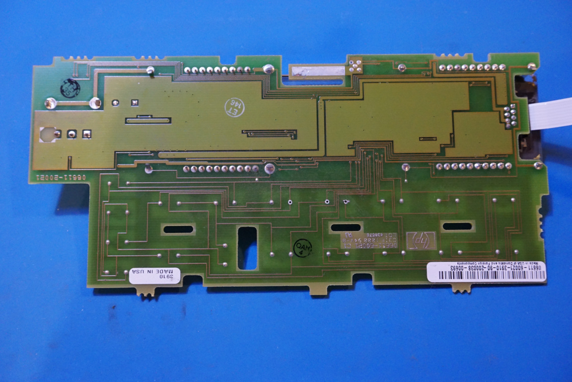
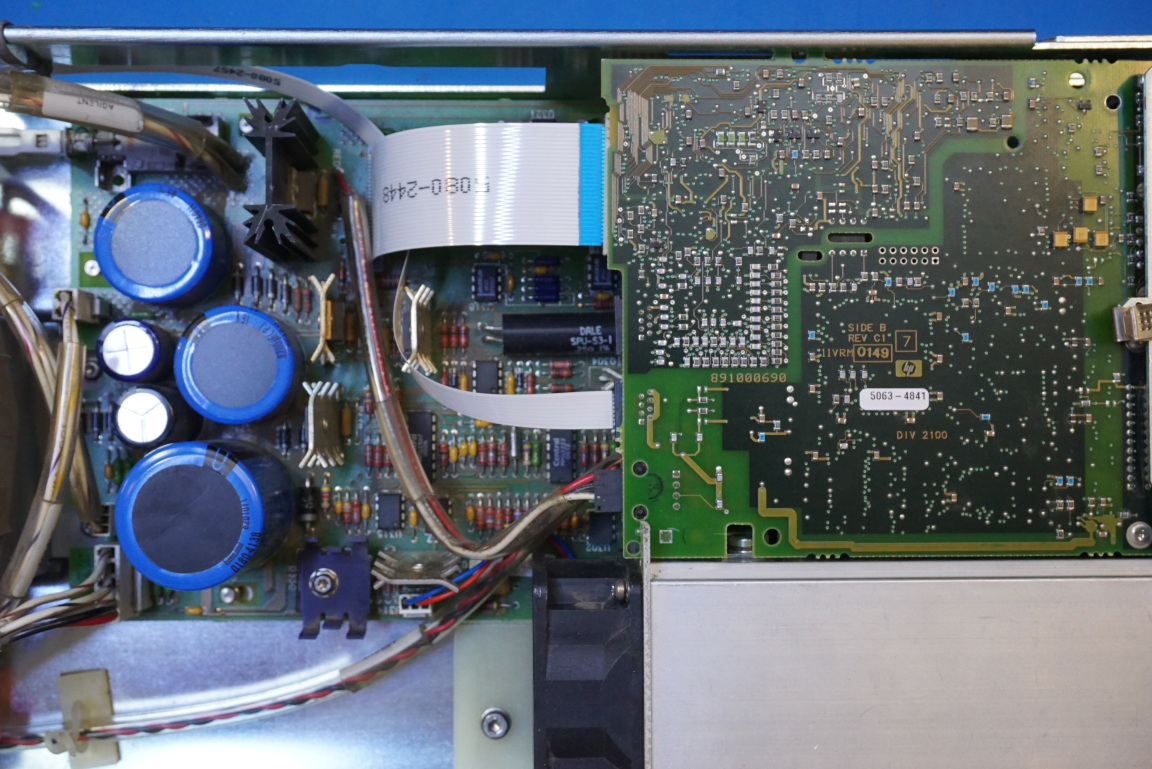
The unit has two main circuit boards. The top board contains all the digital circuitry for controlling the power supply and providing both GPIB and RS232 communication interfaces. The main DSP is a TI’s TMS320C32PCM40 processor. The main ADC used is a 16-bit AD677.
|
|
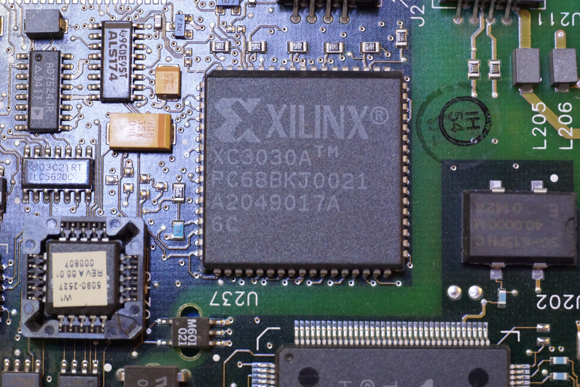
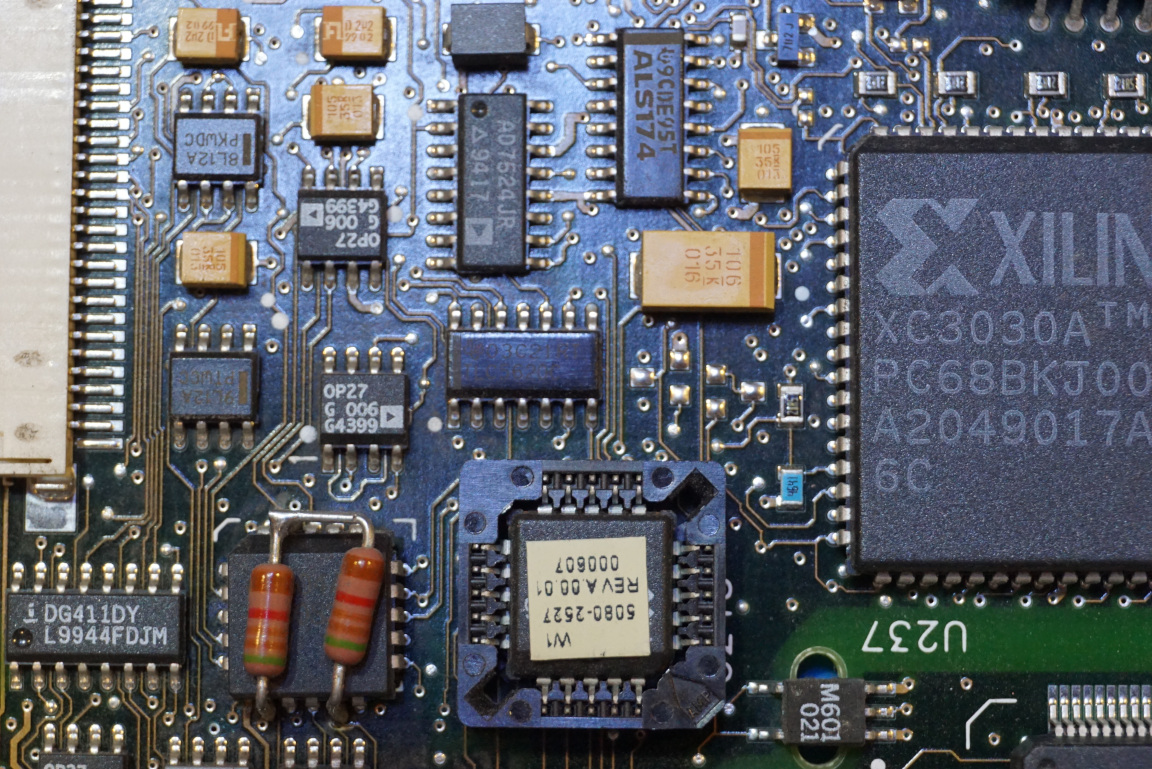
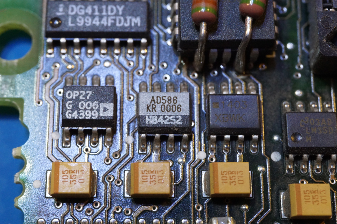
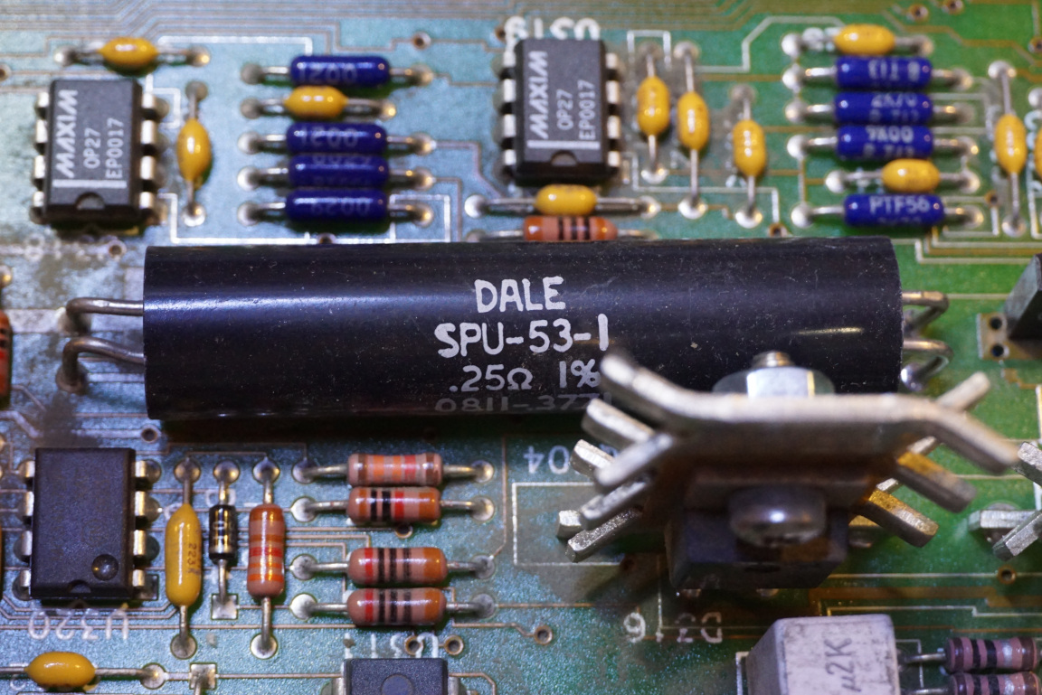
On the same board, there is also a Xilinx XC3030A FPGA and a TLC5620C quad 8-bit DAC. In the picture to the right you can also find an AD7524 8-bit DAC. There are also a couple of OP27 low offset low drift precision OpAmp’s in sight on the board. In fact most of the OpAmps used inside the 66312A are OP27’s.
|
|
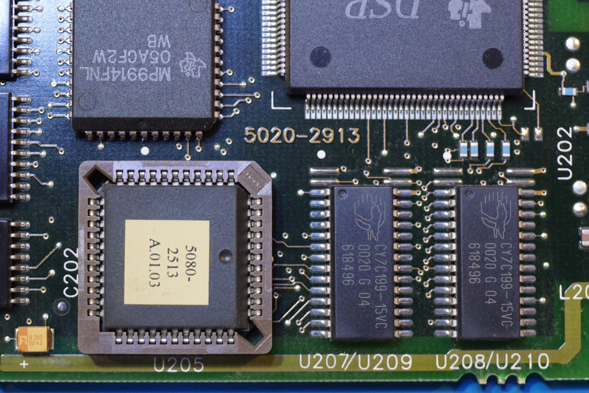
Here you can see a couple of Cypress SRAM chips (32K x 8) used in conjunction with the DSP. And the chip marked MP9914FNL I believe is used for driving the GPIB. The TL16C552FN is a dual asynchronous communication chip with builtin FIFO buffer. An MC145407 is used to drive the serial port given its physical proximity I believe.
|
|
The digital board also houses the main voltage reference for the power supply. The reference used here is an AD586 high precision 5V reference. The “KR” version used here has a maximum 5 mV initial error and a 15 ppm/°C temperature coefficient.
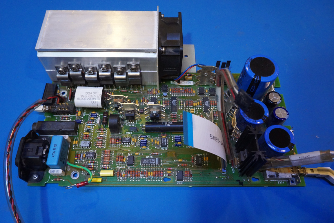
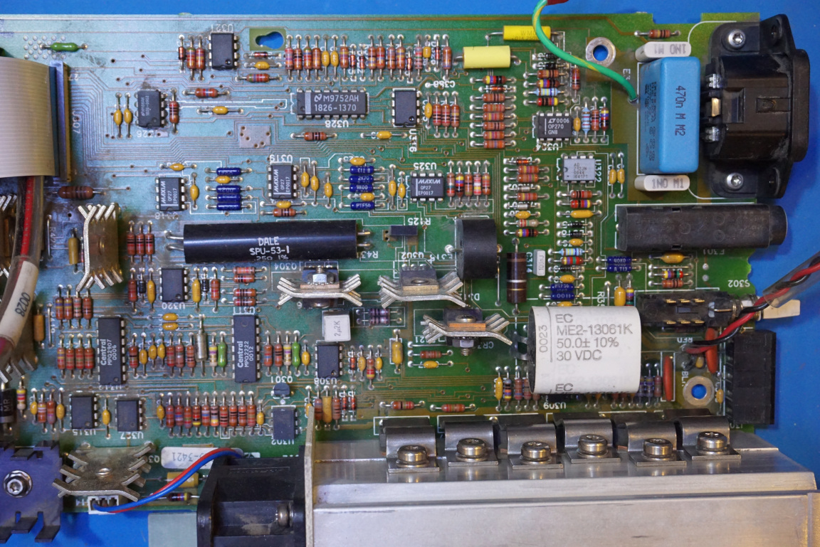
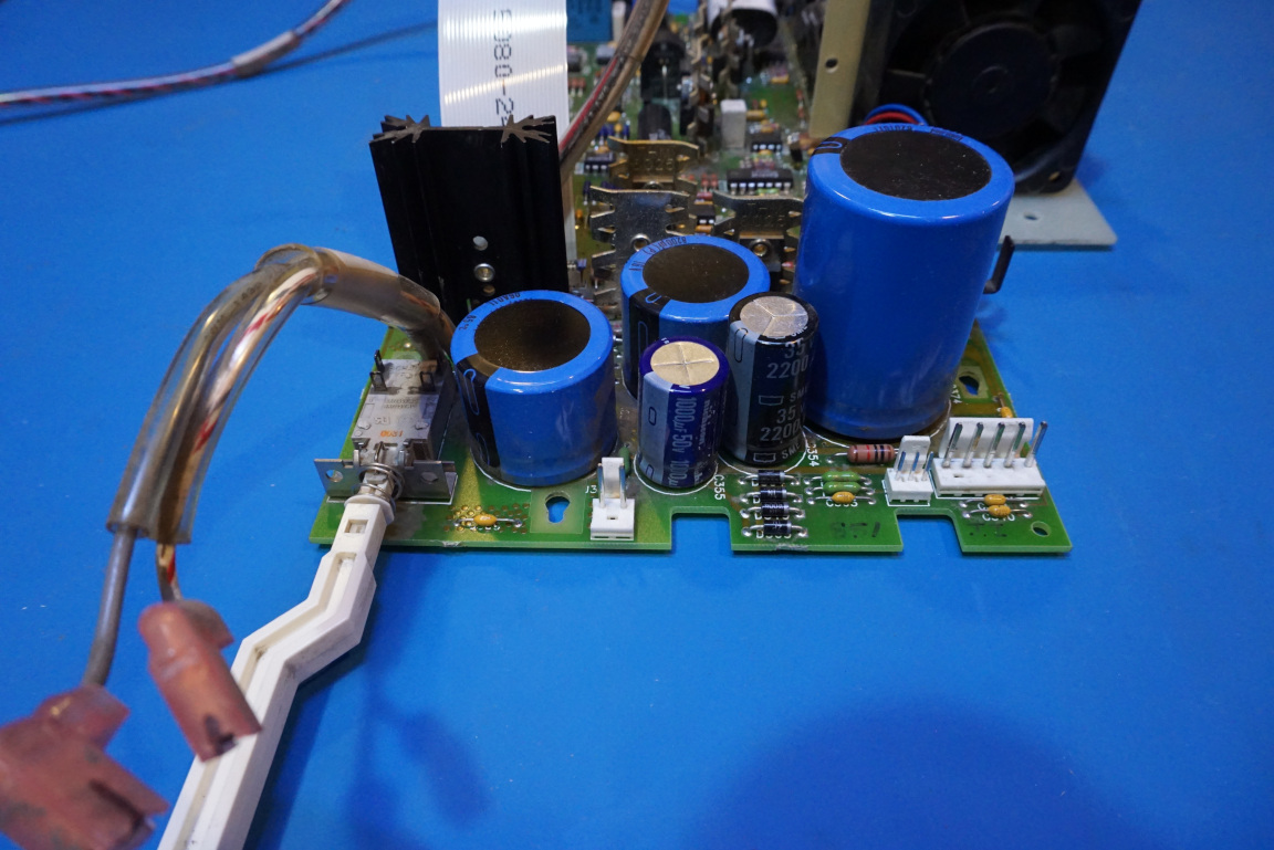
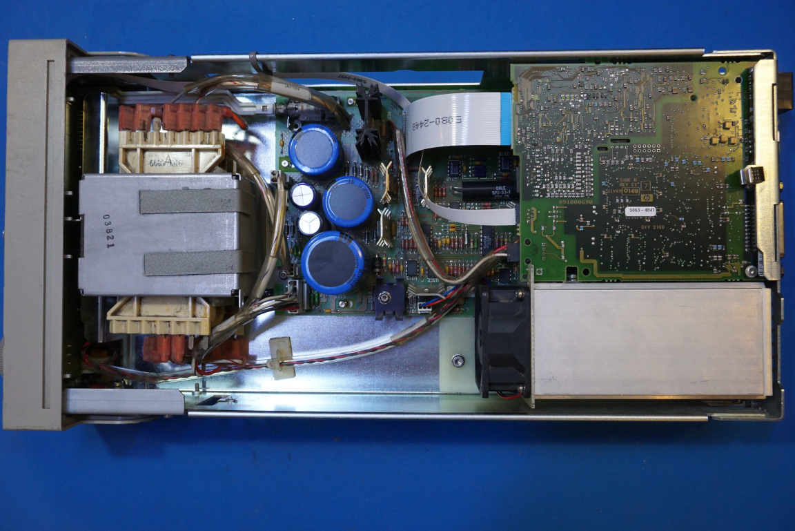
The main board houses the power supply portion of the circuitry. The fan used in 66312A is thermally controlled. In normal operation, it operates at lower power and it will spin up quickly should the heat dissipation rises.
|
|
Here are a couple more pictures showing the board from different angles.
|
|
[adsense]
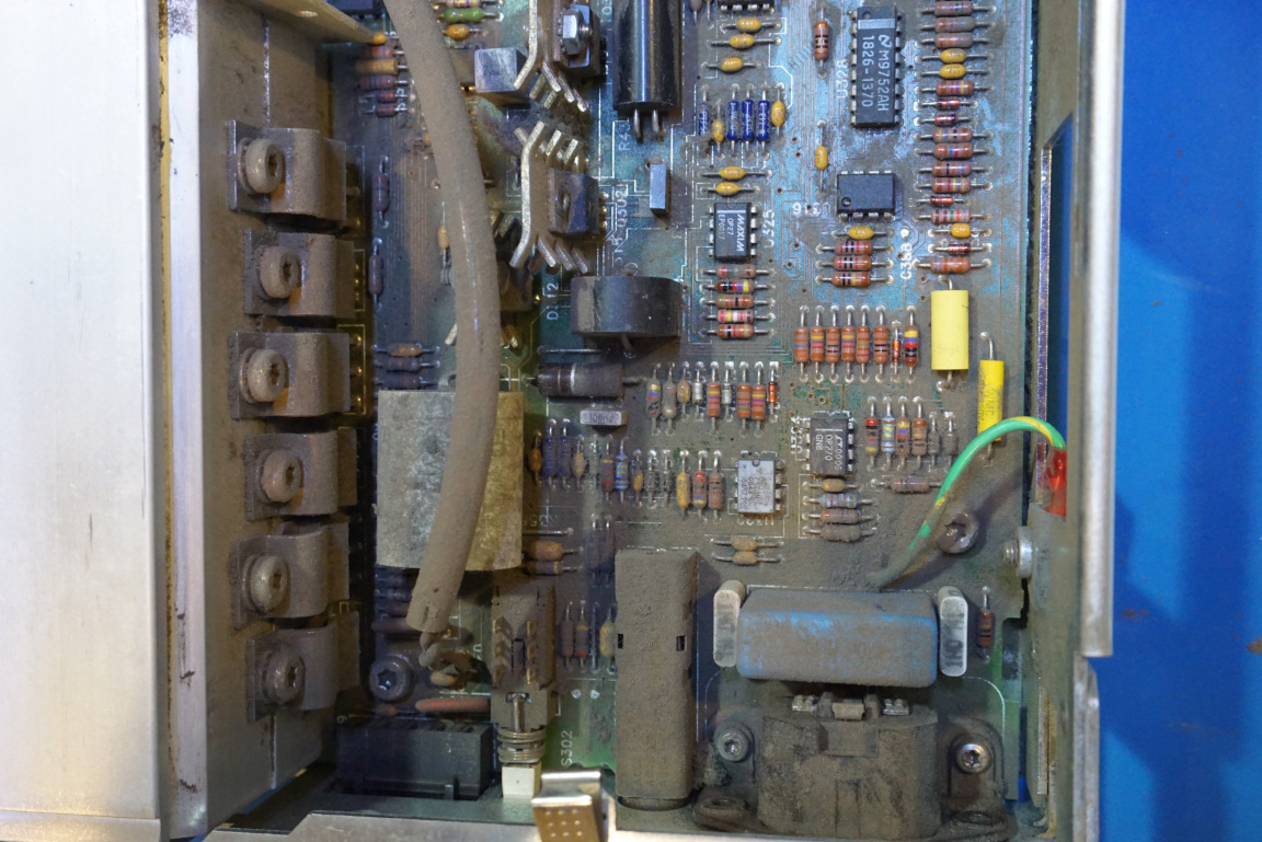
I took the clip off a couple of transistors to see what they are. One is an MTP3055V MOSFET, and the other is a TIP35C power transistor. I suspect that the rest of the power transistors are similar as well.
In the picture to the right below is a close-up of a polypropylene film capacitor on the board. My guess is that it is used for filtering higher frequency component.
|
|
|
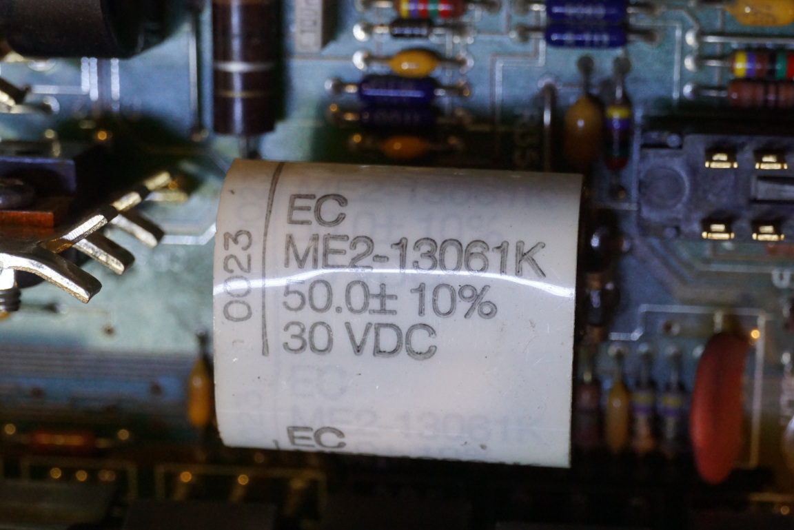
In the picture to the left below, you can see the shunt resistor used for current sensing. A 4-wire Kelvin connection is used due to its small resistance. In the picture to the right you can see a current transformer which is presumably used to pick up the AC component for current measurement.
|
|
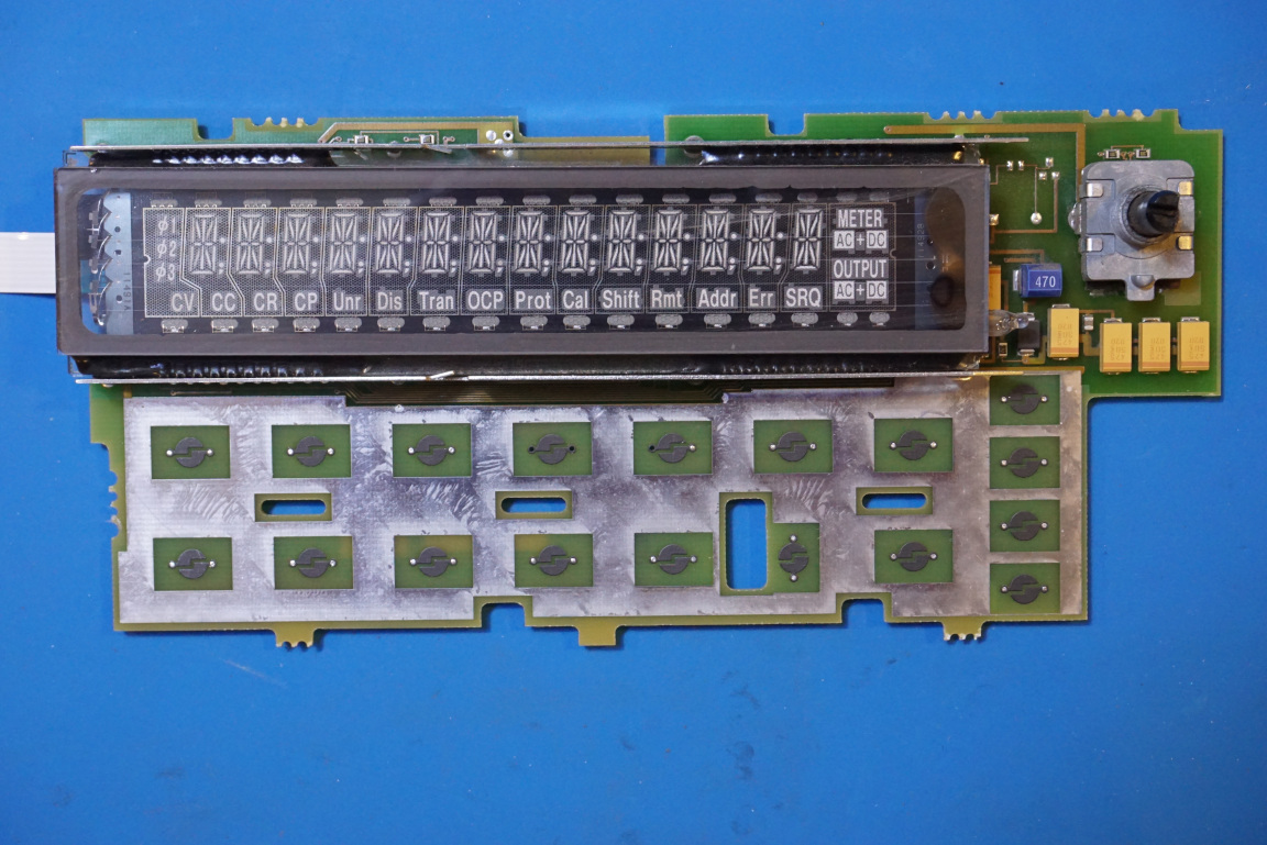
When I initially powered on the power supply, I noticed that the display was quite dim. This is quite common for VFDs as they age. But upon disassembly, I noticed that the display and the filter window were both covered with a thick layer of dust as well which made the problem even worse. The display was noticeably brighter after the dust was cleaned off.
The front panel buttons were also somewhat touchy prior to cleaning. The reason was because those carbonized pads were covered by a layer of dust as well. After cleaning, the buttons became much more responsive again.
|
|
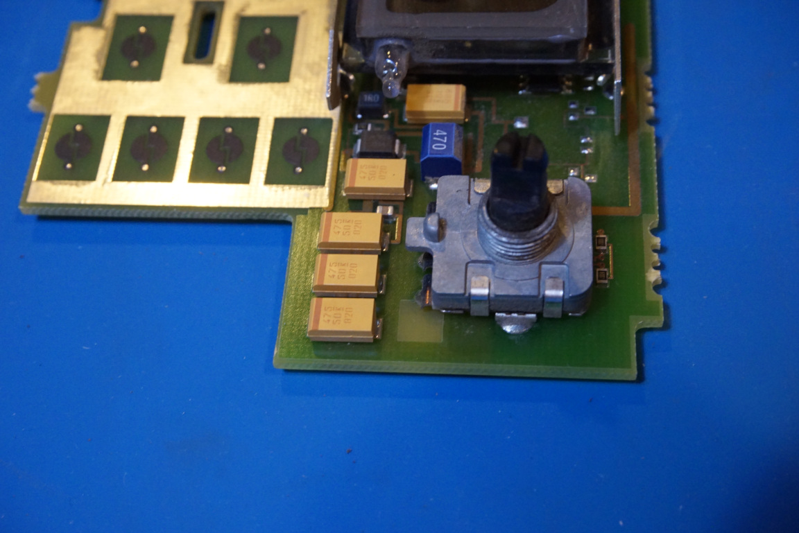
Here is a picture showing the DC/DC converter portion of the circuit for powering the VFD, along with a multi-purpose rotary encoder.
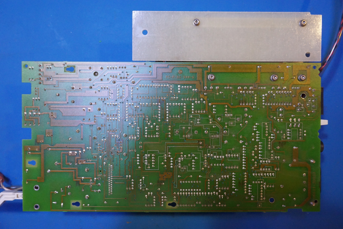
Here are a couple of pictures showing the empty chassis and the power transformer after I cleaned up the interior.
|
|
|
And here are a couple of pictures showing the power supply cleaned up and reassembled.
|
|
In the video below, I tested the current sinking capability of the power supply and discussed each portion of the circuitry as I took the power supply apart. I also showed how to communicate with this power supply via an RS232 terminal using a null modem cable.

