I have been mainly using perf-boards for my electronics projects. Since most of the stuff I build are not very complicated and are one-offs, using perf-boards has been more than adequate. With that said, I did find wiring the headers in my Arduino projects to be a big pain and depending on the number of break-out pins needed to be wired this could be quite time consuming and error-prone as well. Since I have heard many good things about Seeed Studio‘s Fusion PCB Service, I decided to give it a try.
My design goal was to cram as much circuitry as I could onto the 5cm by 5cm board as that is the cheapest option. I also wanted to use a through-hole only design as it is a lot easier for building prototypes. Since many of the ICs I integrate with use either I2C or SPI protocols, I also decided to breakout dedicated I2C and SPI ports. To program the MCU I wanted to have the option of using either the standard ICSP or via serial port using the adapter I built.
With these goals in mind, I came up with the following design:
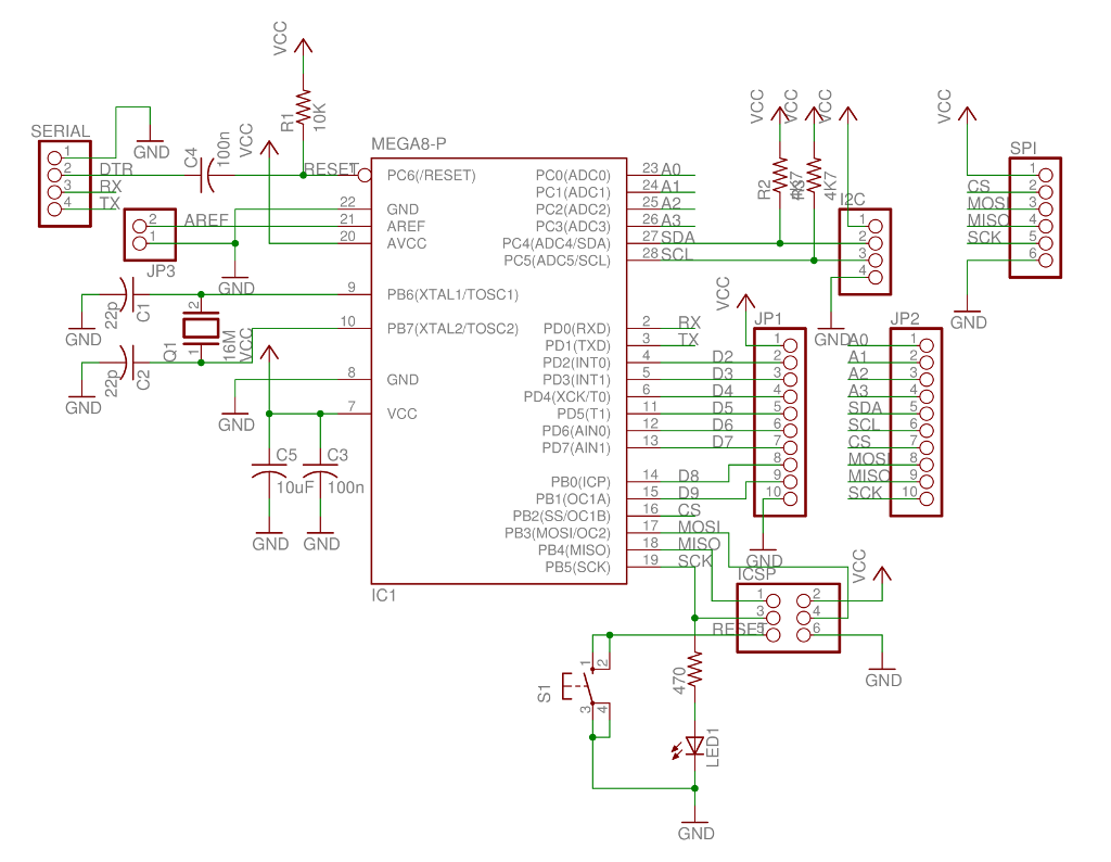
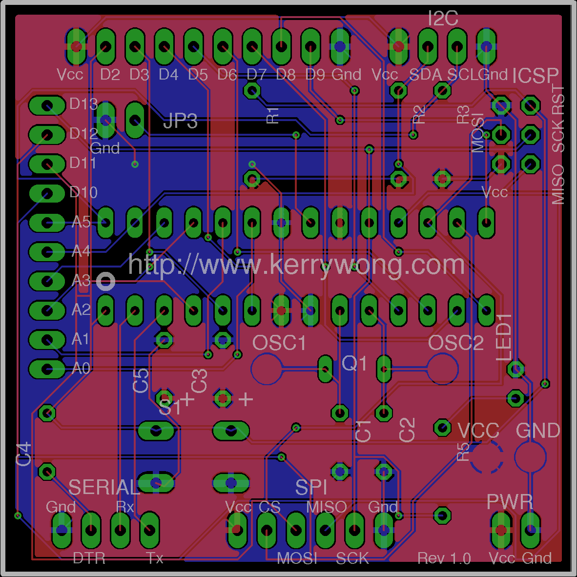
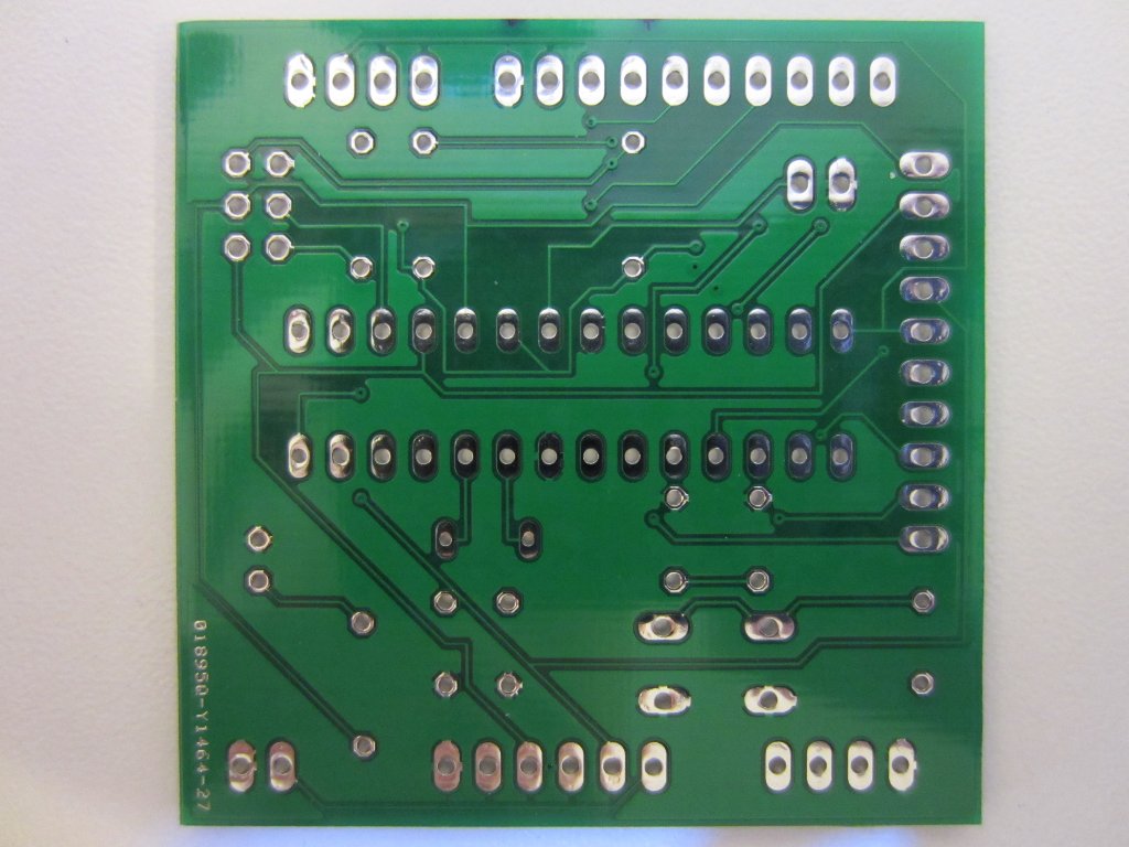
For the PCB design, I basically just chose the maximum design area to be 5cm x 5cm. I also debated whether to add mounting holes or not. At the end I decided to go without the mount holes as I rarely use them. By eliminating the mounting holes, I ended up having slightly more space for the headers. Anyway, here is the PCB design (I turned off the outline layer so that the traces can be viewed more easily).
The design files (a zipped file containing .GBL .GBO .GBP .GBS .GML .GTL .GTL .GTP .GTS and .TXT) were submitted on 12/24 last month and three days later the order status was updated to shipped.
The shipping service Seeed uses (Hong Kong air mail) is not the fastest. After three weeks of waiting, I finally received a box from them last Saturday. Packed inside the box is a sealed bubble wrap package which contains my 10 PCBs:
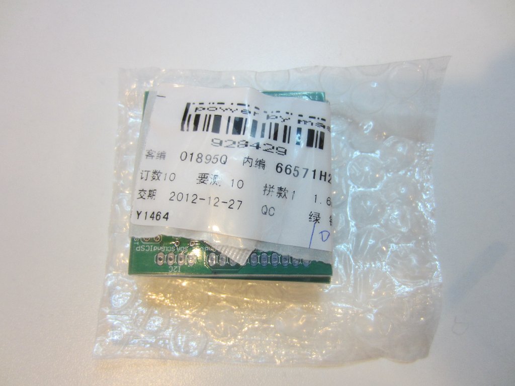
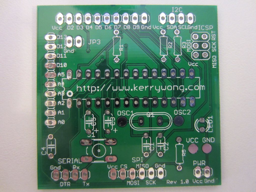
The quality of the PCB is quite excellent (of course for this simple circuit design, this is more or less to be expected), the silk screen looks pretty decent as well. It does appear that the some of the font sizes used for silk screen are slightly larger than the ones I specified, but it is close enough. According to Fusion service’s website, the boards are supposedly 50% e-tested. The probe marks on some of the test pads suggest that this is indeed the case.
 |
 |
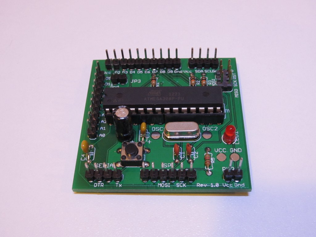
Here is a populated Arduino dev board:
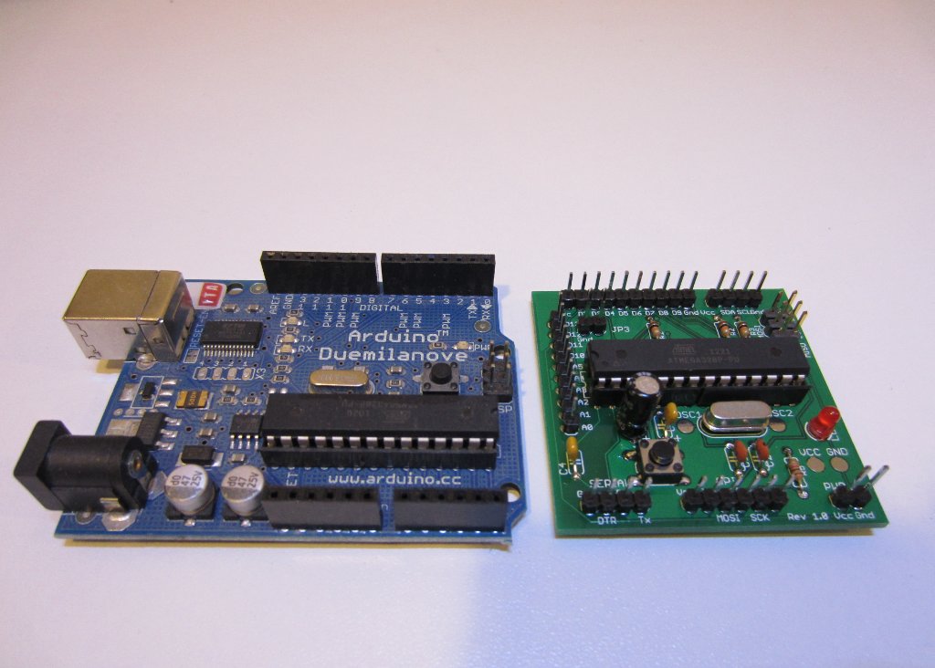
And here is a picture showing the dev board and an Arduino Duemilanove side by side:
Download
Gerber files: ArduinoDev.zip

