In my previous post, I showed my design of a dual tracking ±30V linear power supply. My goal was to use the transformer (28V+28V, center tapped) from an old Deltron W127G open-frame power supply and build a lab supply that can be digitally adjusted in both constant voltage and constant current modes. I also wanted each of the channels to be able to deliver up to 10 Amps of current so that I could fully utilize the 540VA transfomer from the W127G.
The following is the finalized schematic for the positive power supply portion (pretty much identical to the schematic I used in my simulations earlier). Here, I used four TIP35C‘s in parallel as the NPN transistor in the Sziklai pair. Because the input voltage is fixed at roughly 30V under maximum load, in a dead short scenario the power dissipated in the pass transistors is at least 300W and thus four transistors are needed to be able to share this worst case load. If you are building a power supply that is rated for just a couple of Amps, you can use just a single power transistor. I also added a buffer between the DAC and the voltage control loop OpAmp (IC1A) to improve stability. Because the digital/analog converter is not isolated, using a buffer between the DAC and the control point can greatly reduce the risk of damaging the DAC or the MCU should one of the OpAmps fail during operation. Similarly, a voltage follower was also added to buffer the current setting output from IC1B. The protection diodes were included to protect the inputs of the OpAmps during large voltage swings in transient events (such as power on).
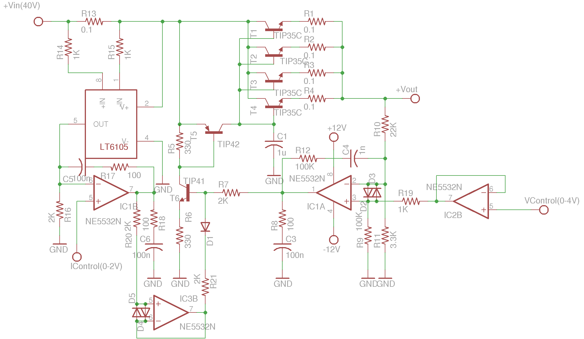
The temperature stability of the regulated output voltage is largely dependent on the temperature coefficients of the resistor divider R10 and R11. As I explained previously, the output voltage is determined by:
\[V_o = \frac{R_{10} + R_{11}}{R_{11}}V_{Ctrl}\]
So using resistors with similar tempco characteristics and low tempcos is preferred if low output drift is desired. Similarly, the resistors used in the current amplifier (R14-R16) along with the current shunt resistor R13 need to be high accuracy and low tempco reistors as well if precise constant current setting is required.
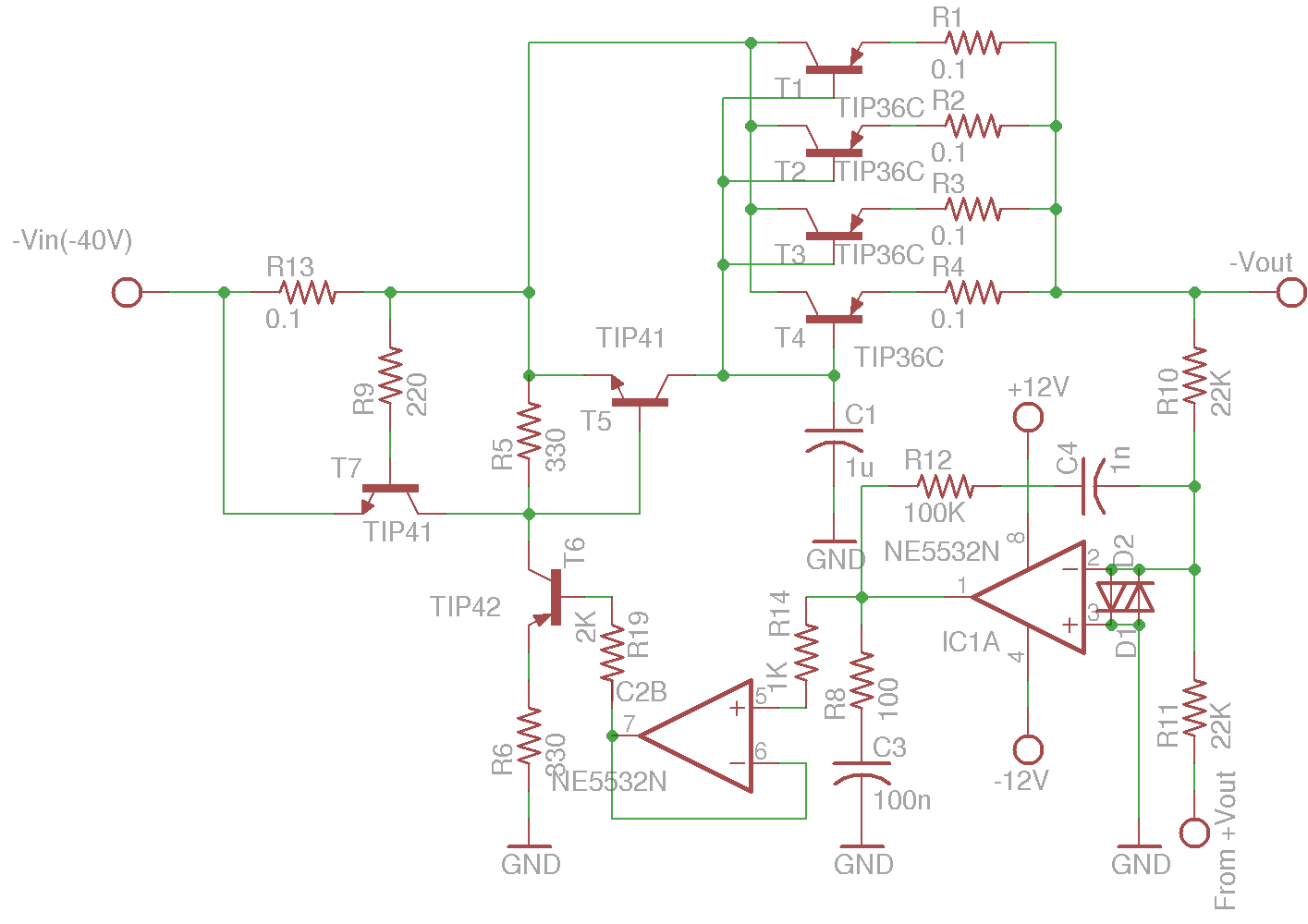
The schematic for the negative power supply portion is shown below. Again, the main differences between this finalized schematic and the one I used in simulation previously are the paralleled pass transistors and the buffered tracking output. As I mentioned before, for accurate tracking performance we only require that R10 and R11 to be equal in value. And as long as they are chosen from the same batch (i.e. same tempco) their temperature drifts can be largely canceled out when they are thermally coupled (e.g. placed side by side). The negative portion of the circuit does not have the current setting capability for reasons I explained earlier, rather the maximum supply current is limited by the Vbe of T7 and the value of R13. For the values given, the current limiter starts to kick in when the load current reaches around 7A. The load current will continue to increase slowly if the load is increased after this point and will plateau at around 10A when the load is completely shorted.
Most modern power supplies utilize two separate transformer windings for the two output channels and the circuits for each channel (except for the tracking portion) are made identical. This would be the preferred approach as the characteristics of the two channels can be made near identical. But here I am limited by the center-tapped transformer I’ve got.
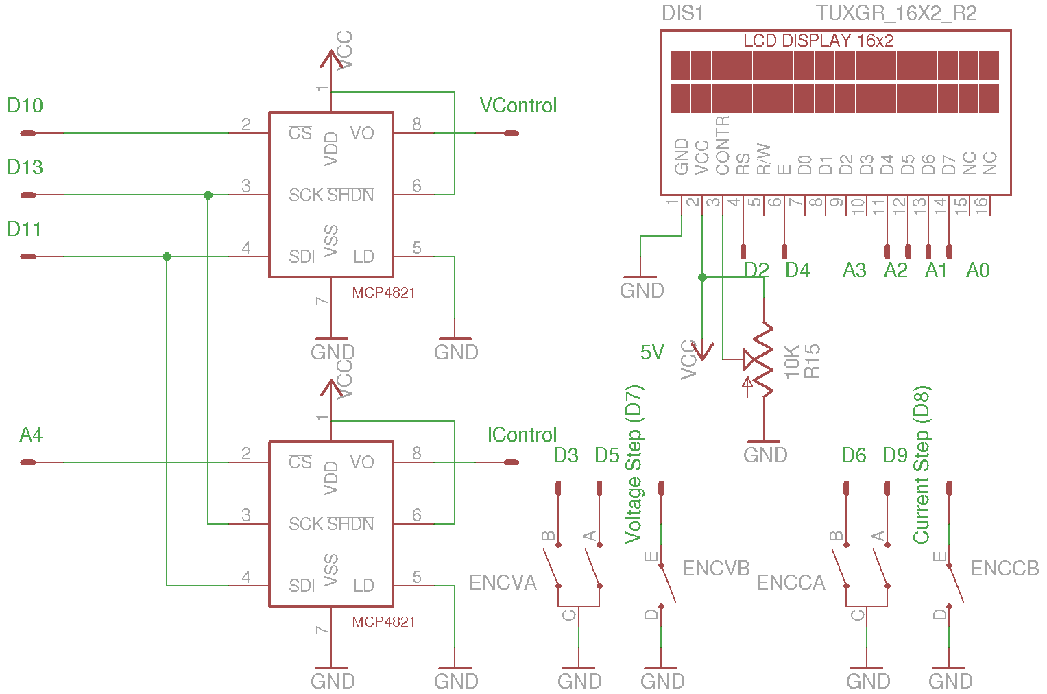
I used two MCP4821‘s to drive the voltage control OpAmp and the current control OpAmp since I’ve got quite of few of these single 12-bit DAC’s. Of course you should consider using a single two channel DAC such as MCP4822 (see my code examples) if you are buying new parts, using a single two channel chip can free up a pin for the chip select and you can use it for other purposes. Voltage and current limit adjustments are achieved via two encoders. The encoders I used also have buttons built in, so as with my electronic load design, by pressing the buttons you can change the adjustment ranges between fine and coarse (x1, x10 and x100 per step).
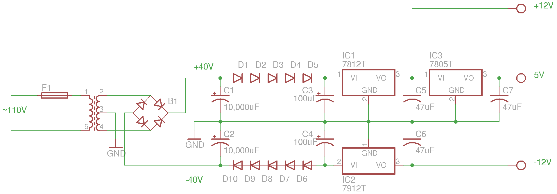
Here are the auxiliary power supply circuits. The ±12V rails are used for the OpAmps and the +5V rail is used for the MCU and DAC. The diodes are needed to drop the input voltages that go into the three terminal regulators to be within the maximum allowed voltage (~37V).
| [adsense] |
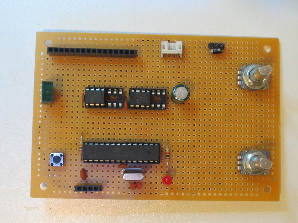
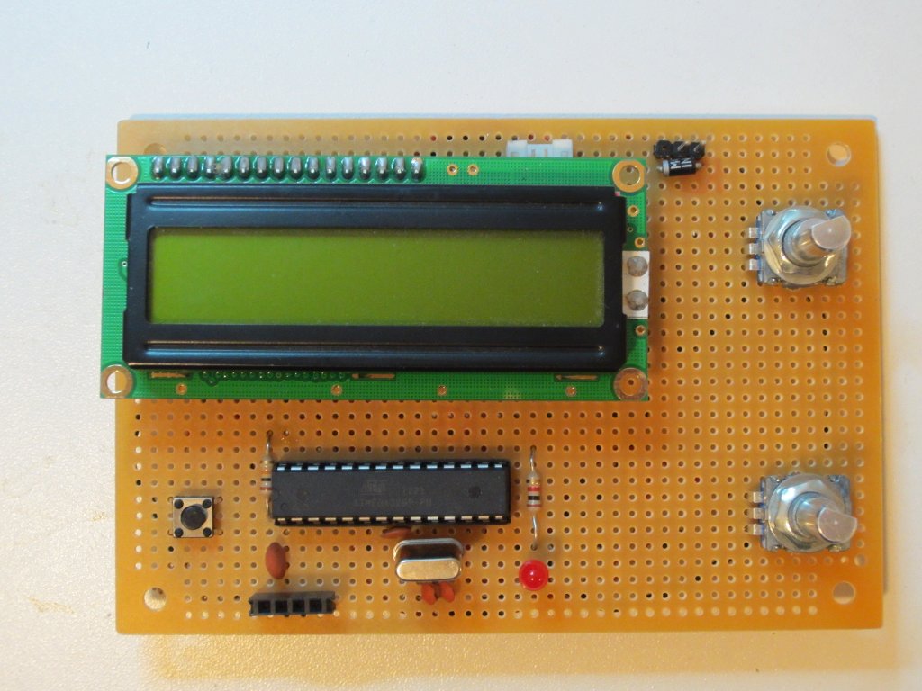
Here are a couple of pictures of the MCU/DAC board. The microcontroller I used is an ATmega328P and the pin designations shown below are compatible to the standard Arduino pinout. The full code listing can be downloaded towards the end:
|
|
And here is a picture showing the overall layout of the power supply. The transistors for the positive channel are mounted towards the upper edge and the transistors for the negative channel are mounted towards the bottom. The two regulators for the ±12V voltages are located towards the center left (I used LM317/LM337 instead of 7812/7912 since I have plenty of them) and the 5V regulator is mounted on the other end of the board (hidden under the MCU board assembly).
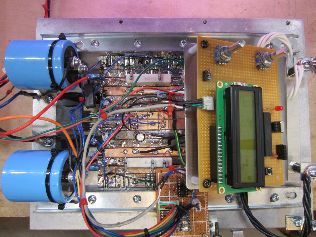
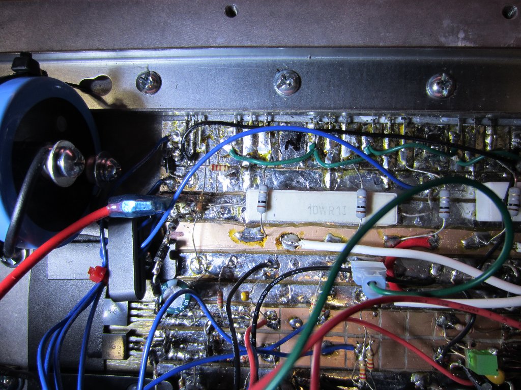
The picture on the left below is a closeup of the OpAmp board. Towards the back on the right you can see the aforementioned 5V regulator. The picture to the right is a closeup of the positive supply portion. Underneath the metal bar are the power pass transistors, you can infer their locations by the placements of the four 0.1 ohm resistors. The leftmost transistor is a TIP42 (T5). Technically speaking, it does not require heat sink. But it is convenient enough to put it along with all the other power transistors.
|
|
So, does it work? For those who are impatient, here’s a picture showing the power supply set for the maximum output voltage and maximum current limit:
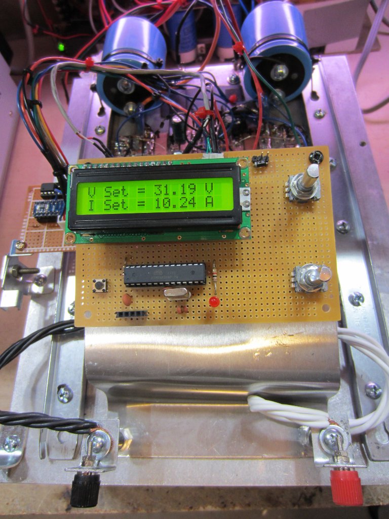
In my next post I will take some measurements and take a look at the some specs of this power supply.

