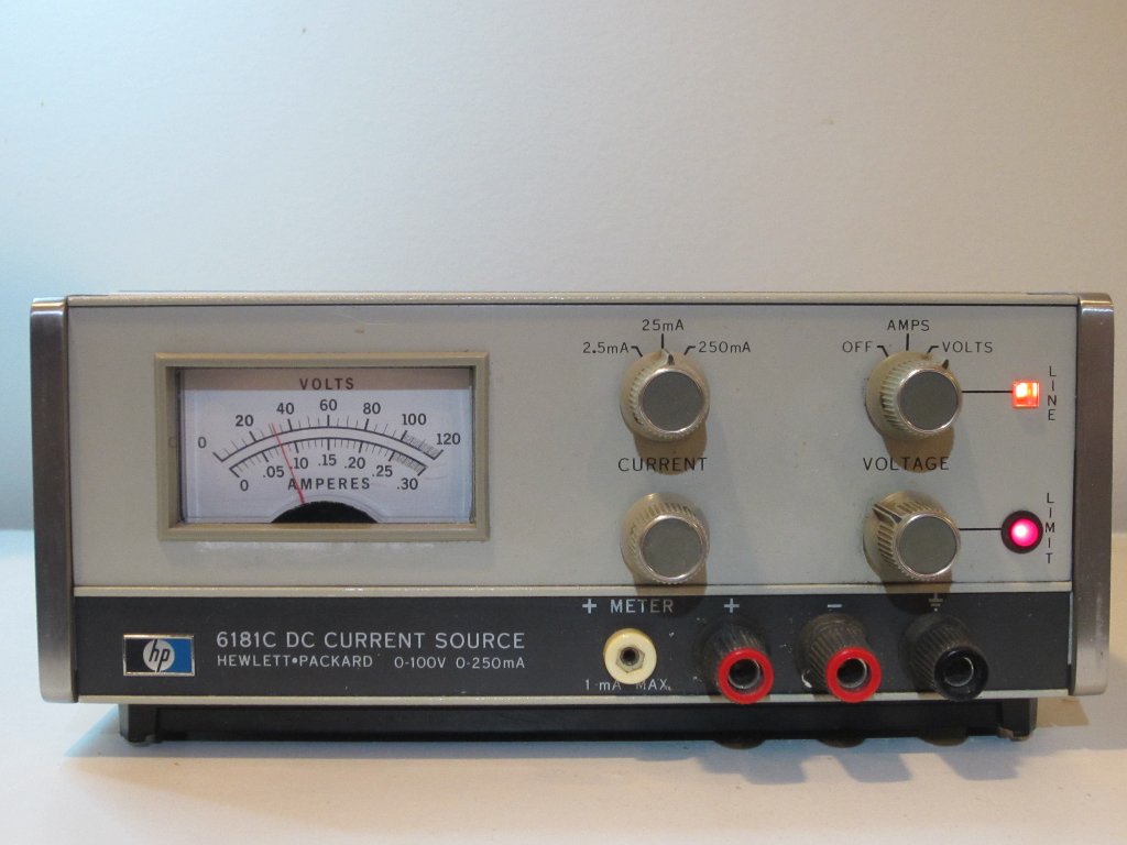
HP 6181C is a lab grade 0 to 250 mA current source manufactured back in the late 70’s and early 80’s. There does not seem to be any pictures on the Internet for this particular model so I thought I would do a teardown here.
Before doing the teardown, let’s take a look at some of its key features. HP 6181C has three output current ranges: 0-2.5 mA, 0-25 mA and 0-250 mA. The output voltage limit can be set from around 0.5 V to all the way to 100 V. The output current can be adjusted via a 10-turn potentiometer and has a set resolution of 0.03% (under 1µA in the 0-0.25 mA range). The output current stability is rated at around 100 ppm, while not top-notch by today’s industry standard but remains quite impressive for hobby use.
The top panel is perforated for optimum heat dissipation. It can be easily slid off after removing the two screws towards the back. Upon removing the top panel, you can see pretty much the entire circuitry. To remove the main PCB, I first removed the 6 screws that hold down the PCB. Then I unplugged the two female headers (one from the front panel and one from the power transistors). The main PCB is connected to the main power supply via a PCB connector towards the back, which requires loosening the side panels and the rear panel before it could be wiggled out. But it was still pretty straight forward.
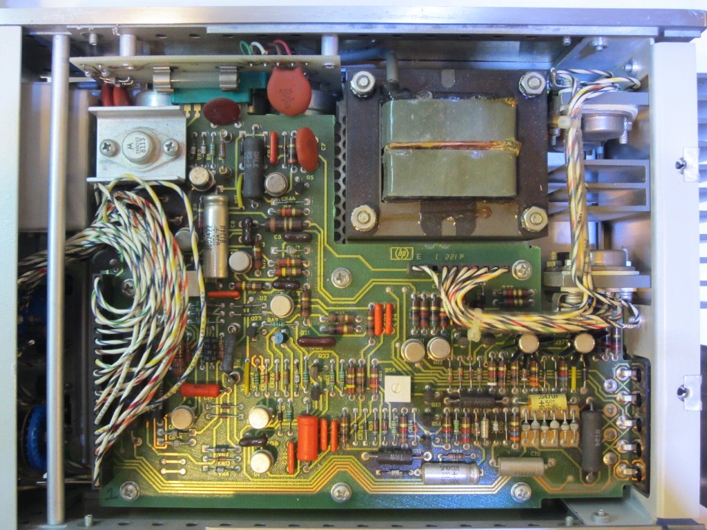
Here are a couple of pictures of the main PCB once it has been removed:
|
|
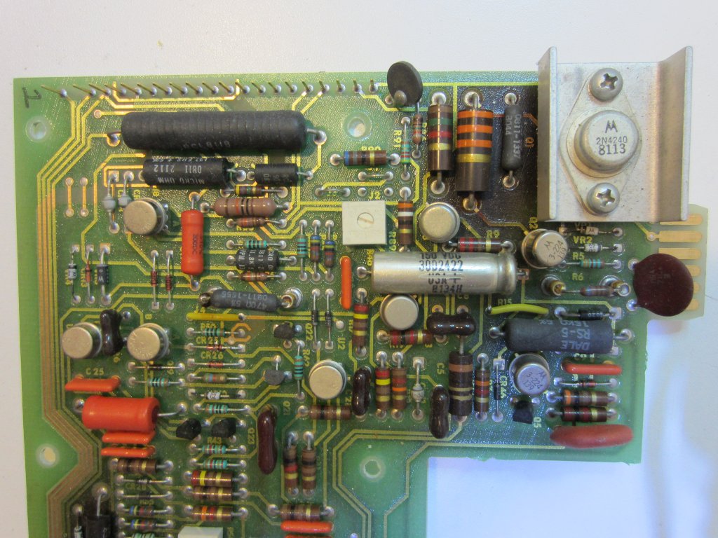
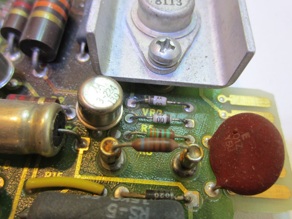
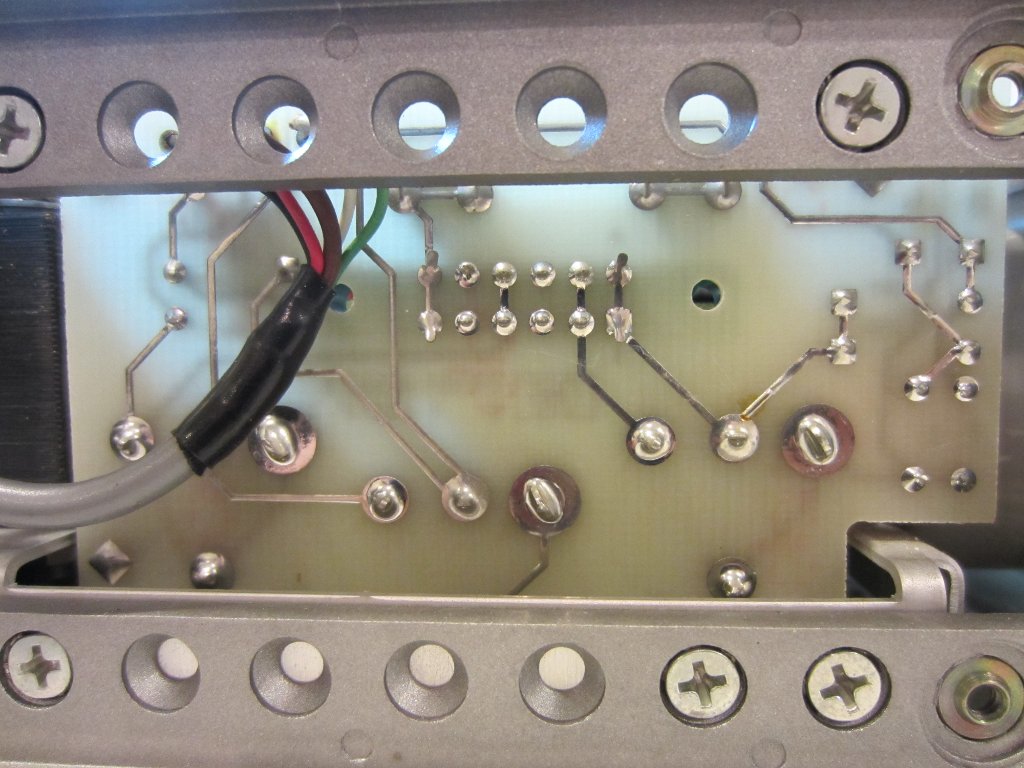
If you look carefully at the close-ups below, you can see that some resistors are soldered on standoffs. This is not to reduce surface current leakage however. According to the service manual, these resistors are the ones that may need to be changed during calibration. Instead of using trim-pots, the resistors are soldered in place with the exact calibrated value. Because there is no moving parts technically speaking, once the current source is calibrated its long term stability is very good.
All three OpAmps are in TO-99 packages. They are general purpose OpAmps (LM301AH) and can be easily replaced if needed to (although, you may need to build custom adapters if you use DIP or SO packages).
|
|
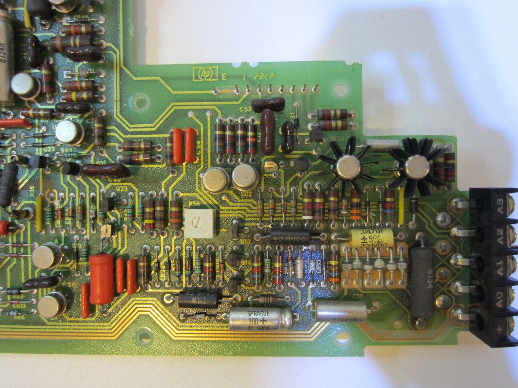
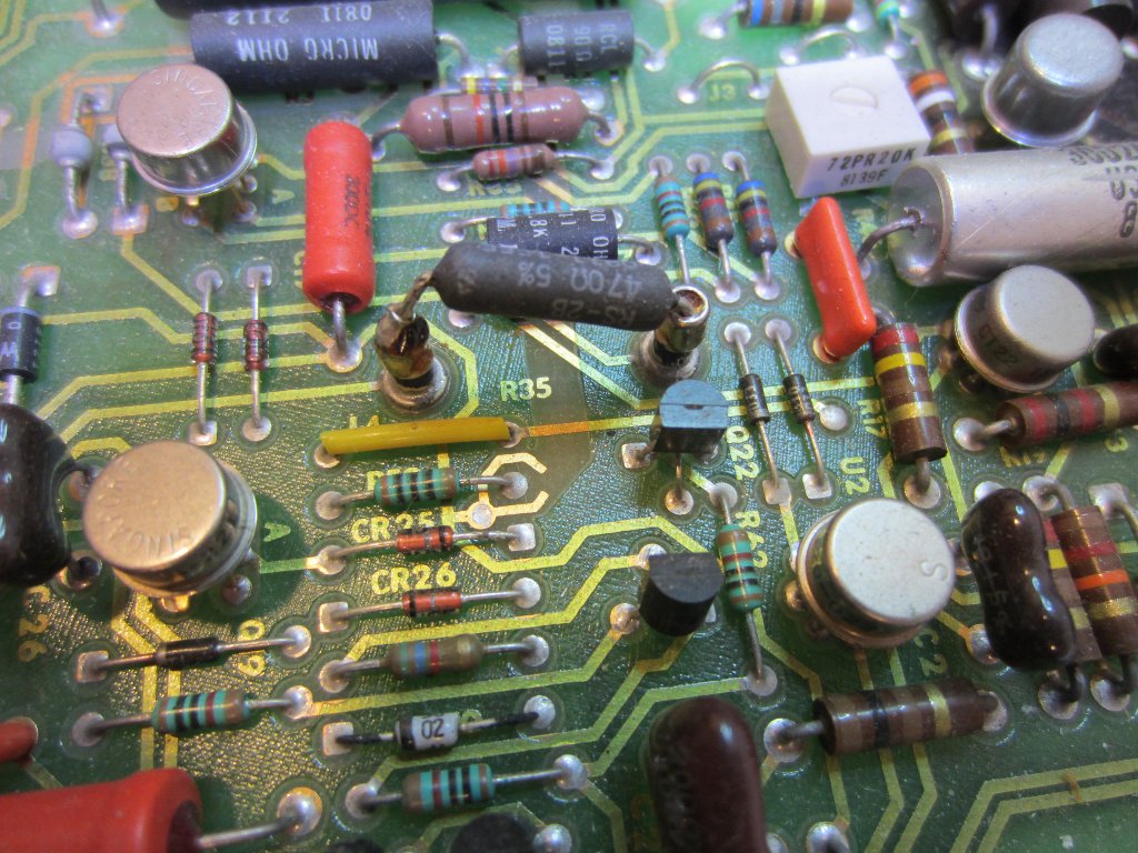
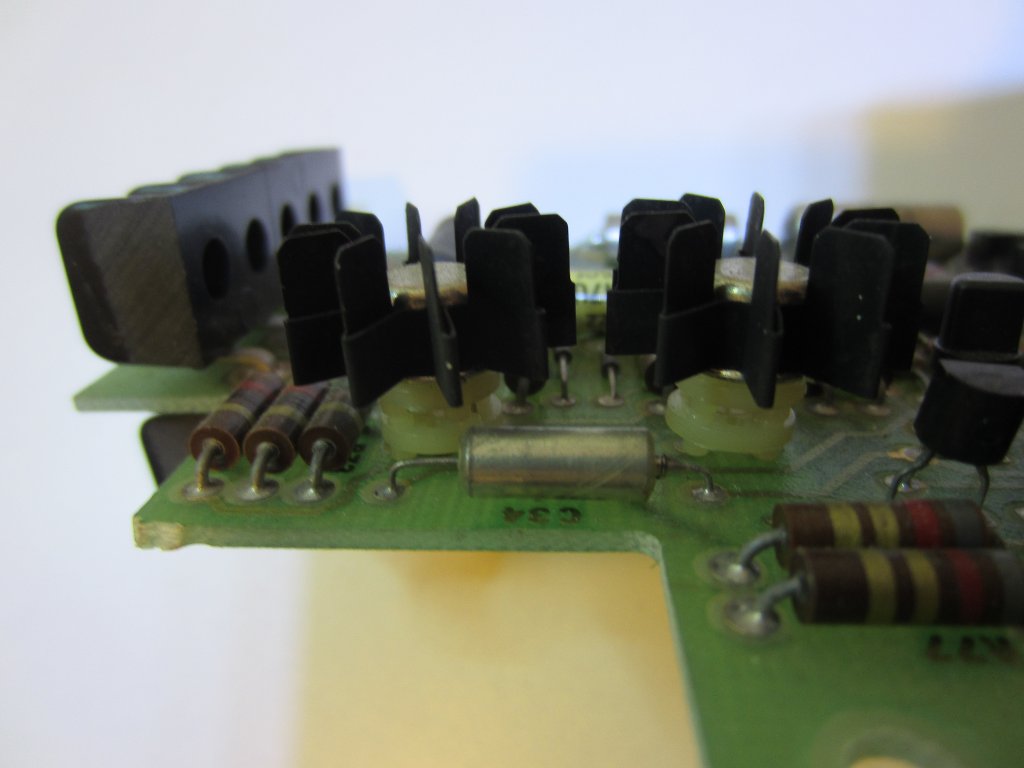
A few transistors have small heat sinks on as you can see in the picture below. Also note the plastic standoffs on these transistors for added mechanical strength.
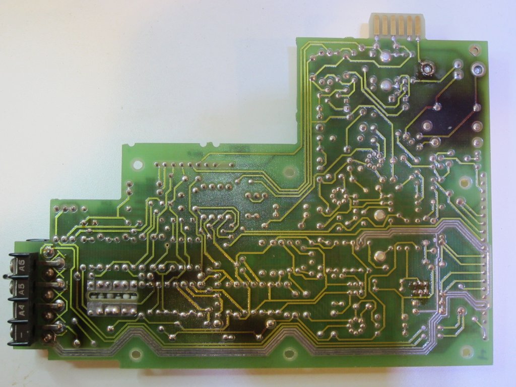
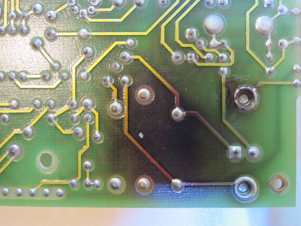
The main PCB is double sided, the picture below shows the bottom layer of the PCB. You can see a couple of dark areas from the reverse side and both areas have power components mounted on the main side. So they are probably caused by prolonged use under heavy load. The age of the PCB in addition to the heating effects may also have contributed to the discoloration as I have never noticed the equipment getting hot.
|
|
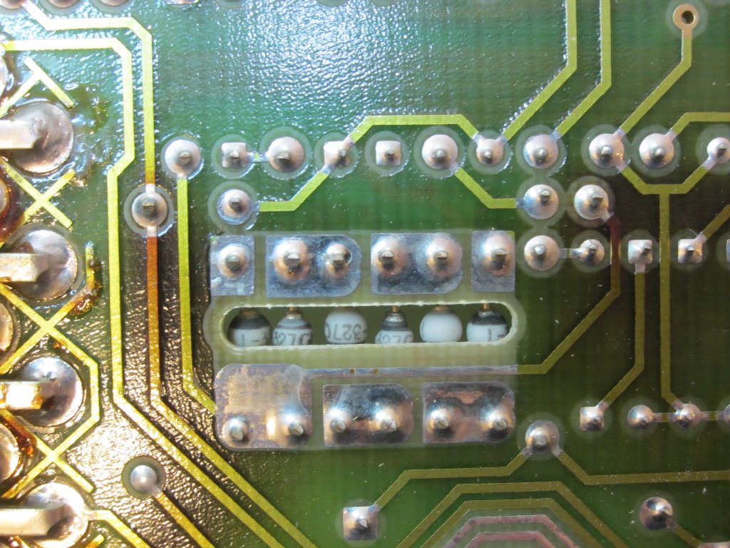
In the picture below, you can see the high-voltage cut-out below the six diodes. Four of these diodes are connected in series to the guard voltage supply.
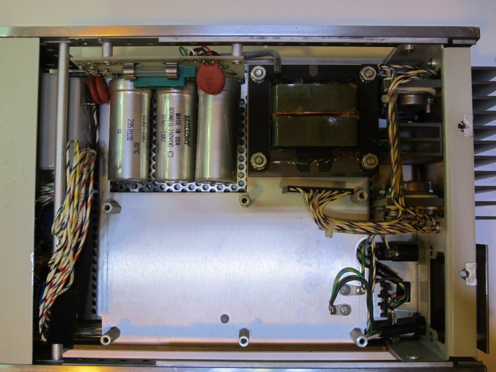
With the main PCB removed, the picture below on the left shows what it looks like inside the case. The bottom aluminum board is elevated from the main chassis, serving as a shield for the power connection wiring underneath. The three electrolytic filter capacitors were the originals, dated back from 1981. Yet they still hold their capacities very well. From the picture on the right, you can see the PCB header for the power connection.
|
|
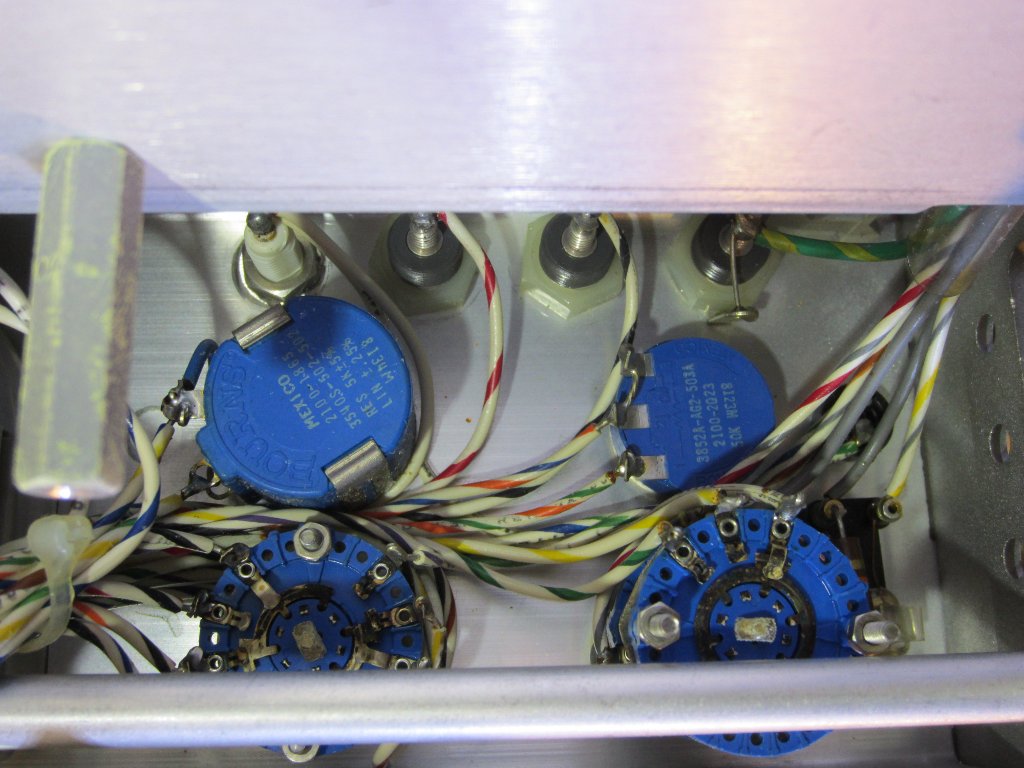
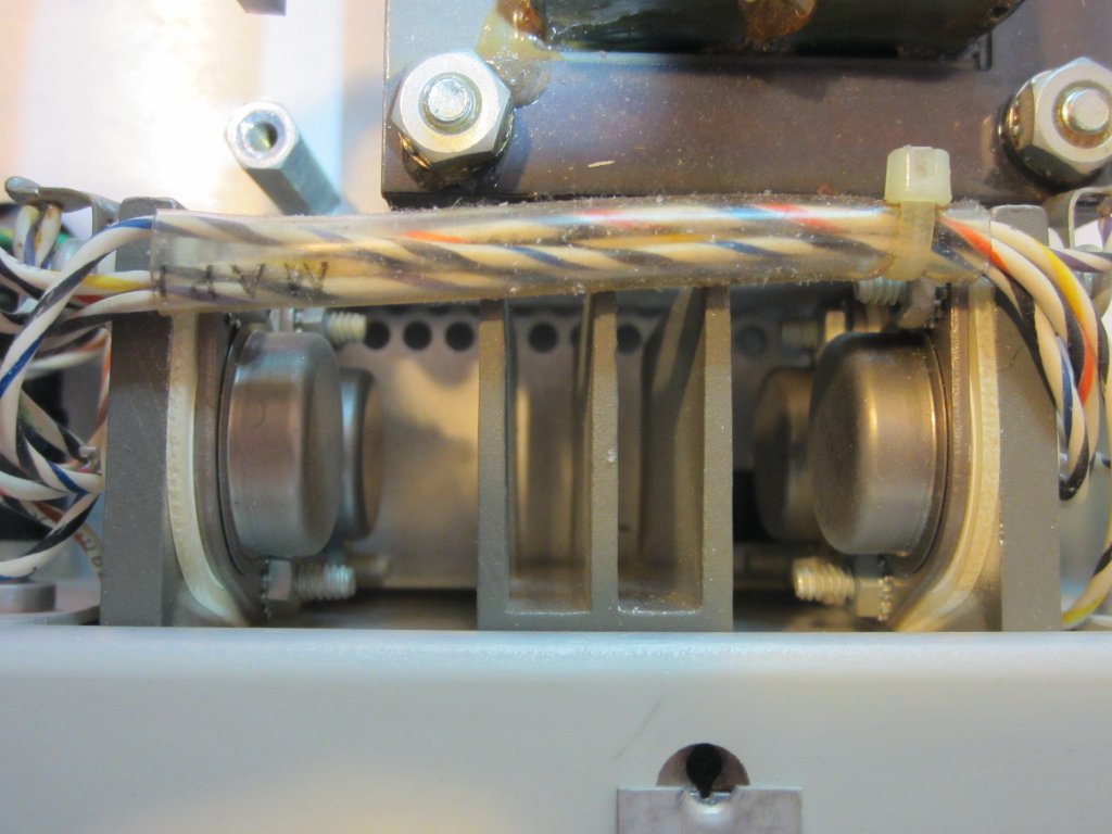
The picture on the left below shows what’s on the other side of the front panel. The larger 5K potentiometer is a 10-turn precision pot that sets the output current and the smaller 50K single turn potentiometer is for the voltage setting. The picture to the right shows the power transistors mounted on the heatsink at the back of the unit.
|
|
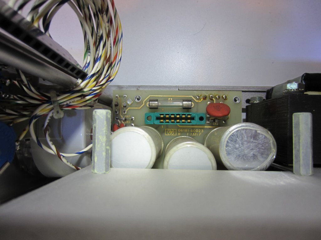
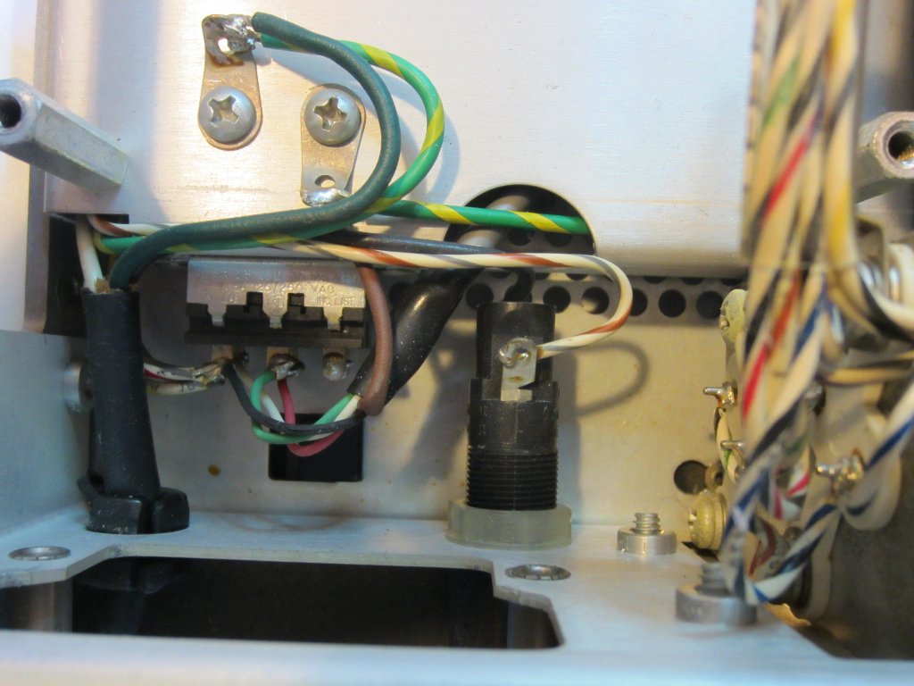
Here is a picture showing the bottom of the power supply PCB where the electrolytic capacitors are mounted. You can also see the nicely machined aluminium support bars. Back in the old days, they certainly did not skimp on material and the whole unit was built rock-solid like a tank. The picture on the right shows the mains voltage selection switch and the main fuse. They are located at the bottom towards the rear panel.
|
|
Perhaps one of the reasons I think this old HP current source is perfect for hobbyists is that it is entirely analog and all components are readily available today. So it can be easily repaired and calibrated if it is needed.

