In my last post, I showed my LED backlight mod of the HP 8642B synthesized signal generator. And during the process, I also showed some pictures of the A1 (keyboard and LCD) module and A2 (modulator) module alone with an intriguing Easter egg message in the firmware. In today’s post, I will do a full teardown of each module and take a closer look at what’s inside.
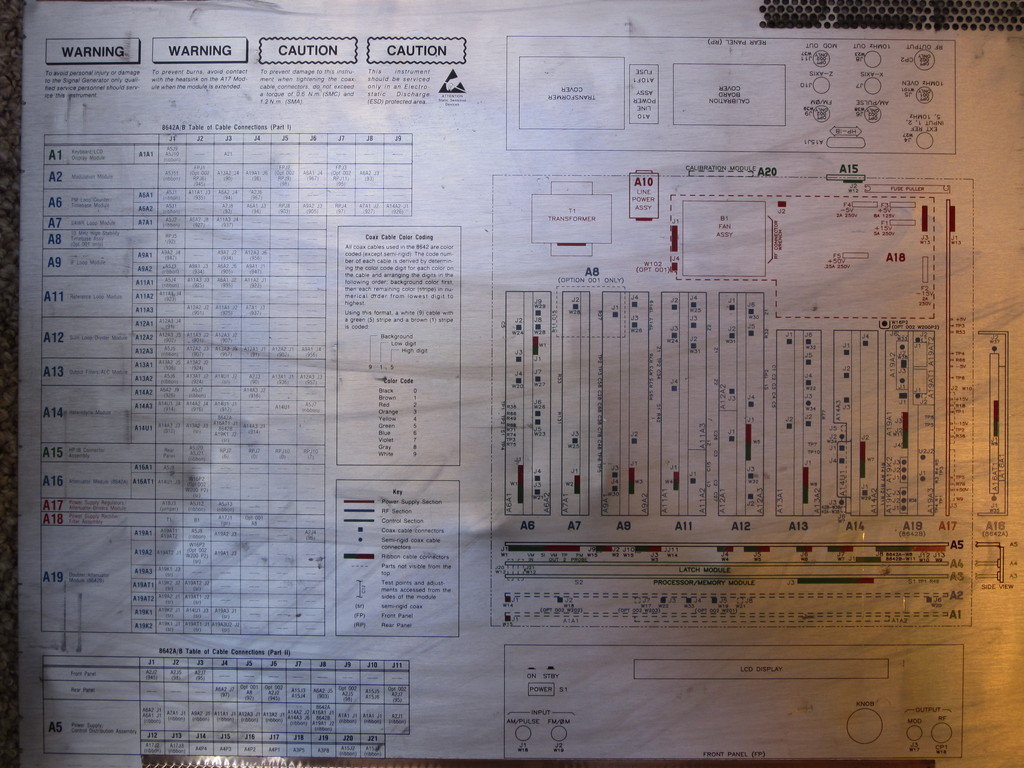
Since I had already posted the pictures of the A1 and A2 modules, I will not repeat them here. Here’s a picture showing the reverse side of the top cover. It has a detailed layout map of what’s inside the unit. For this teardown, we will go module by module from left to right (A6 to A17 and then A17).
Also, I am did not take out the fan assembly and the power supply assembly towards the end (A18) since they are pretty standard and not that exciting.
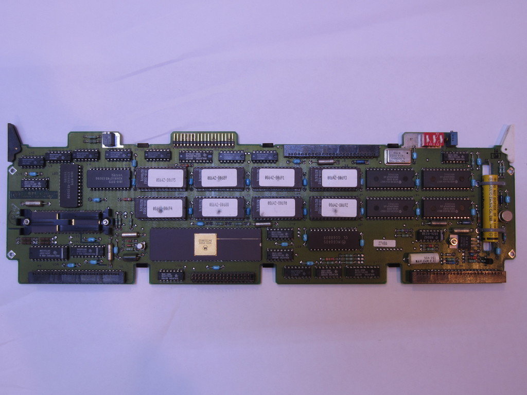
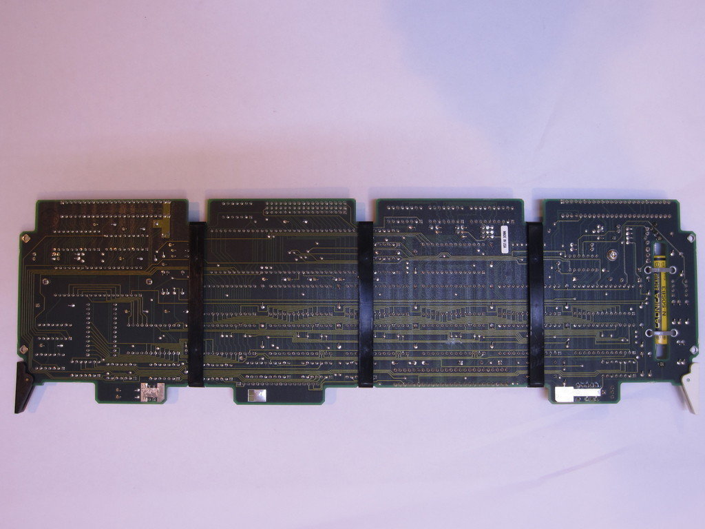
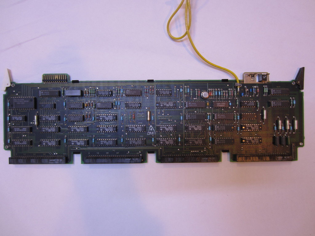
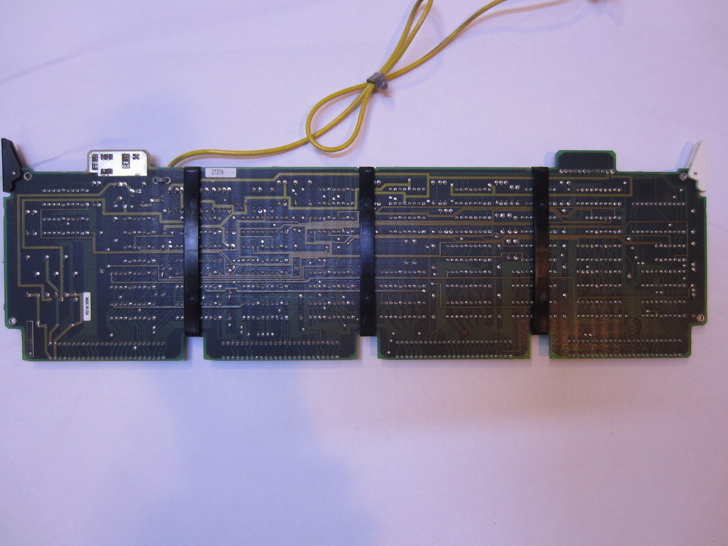
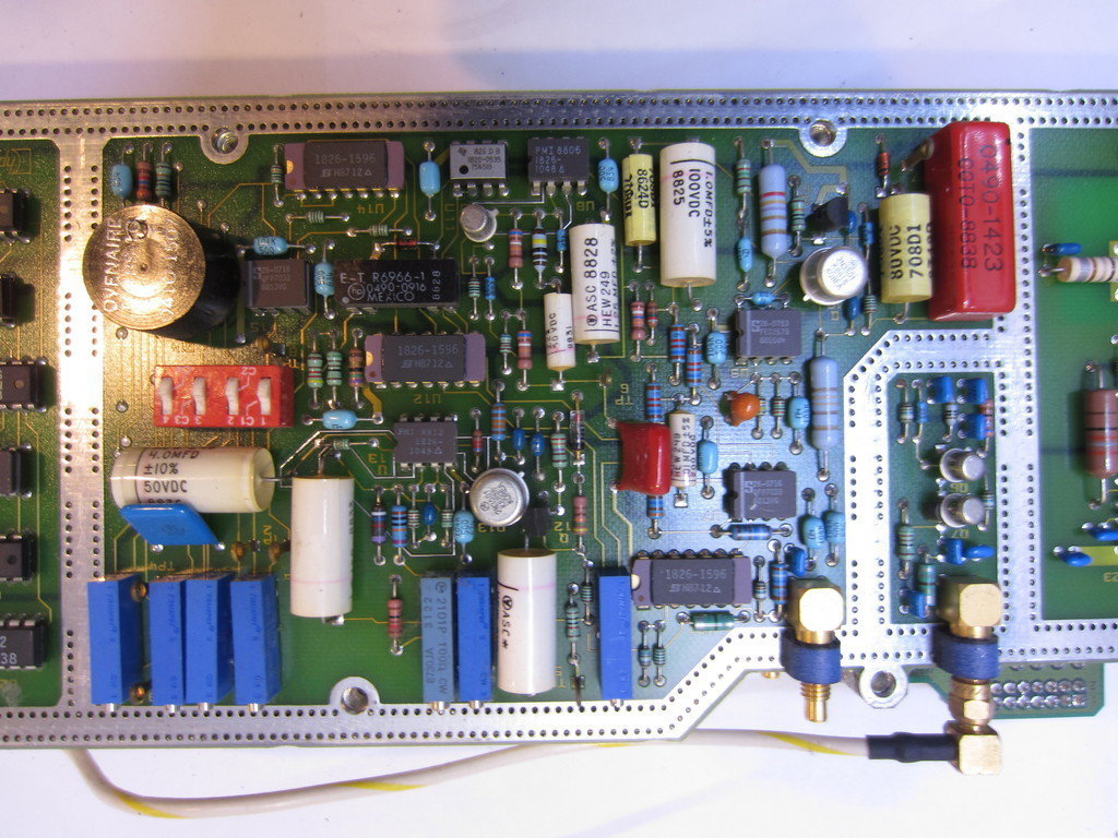
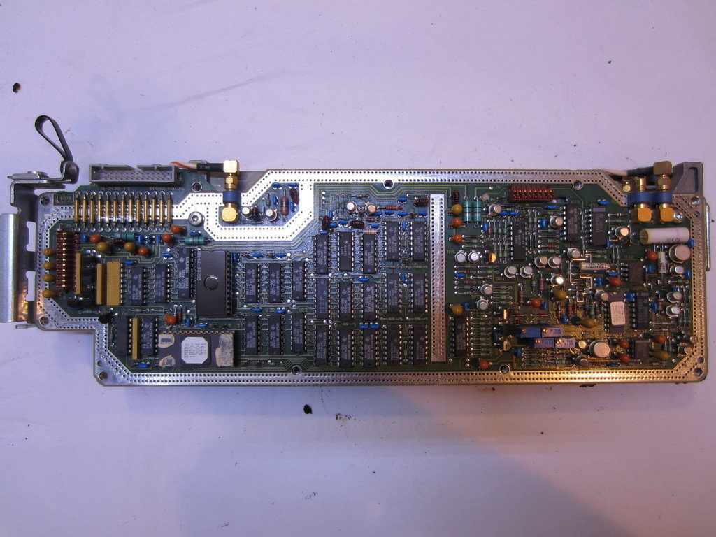
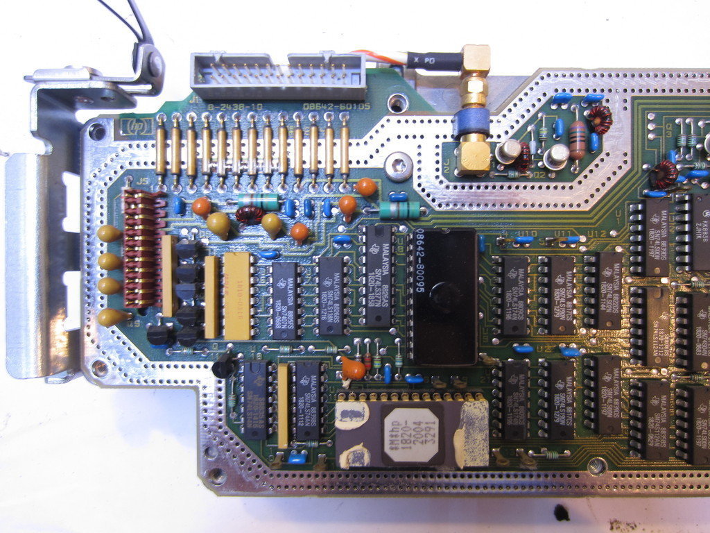
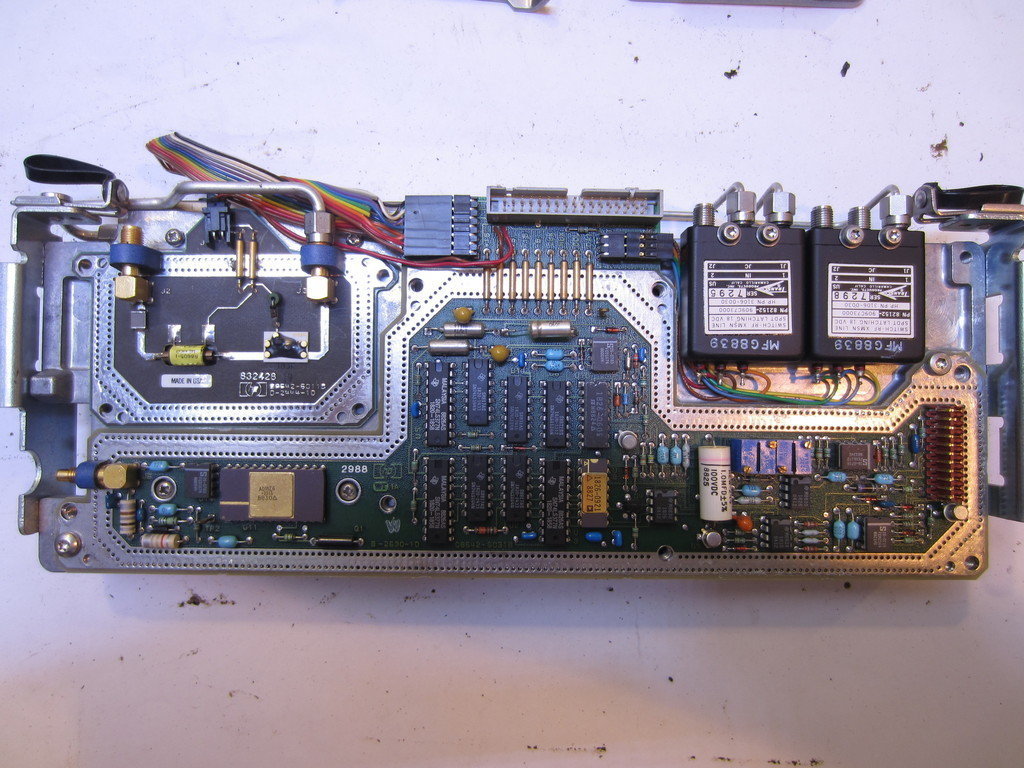
A3 Processor/Memory Module
A3 module sits near the front panel and is pretty easy to remove.
The crystal oscillator frequency used here is 5 Mhz. Take a look at the chip to the upper left of the main processor, the way it is heatsinked is rather interesting.
|
|
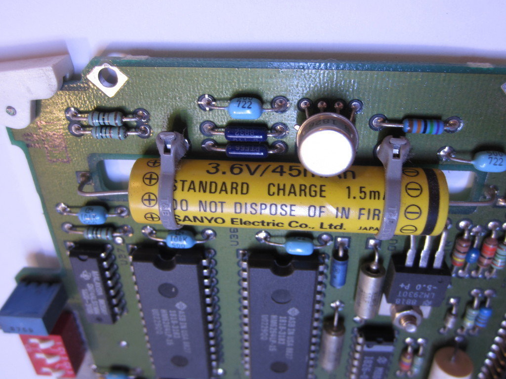
Here is a picture of the backup battery. It is used to retain the settings in the RAM when power is lost. The battery is rechargeable (rated at 45 mAh). Since these units are designed to be plugged in all the time, the battery is designed to last only a short period (e.g. several days) before it is depleted.
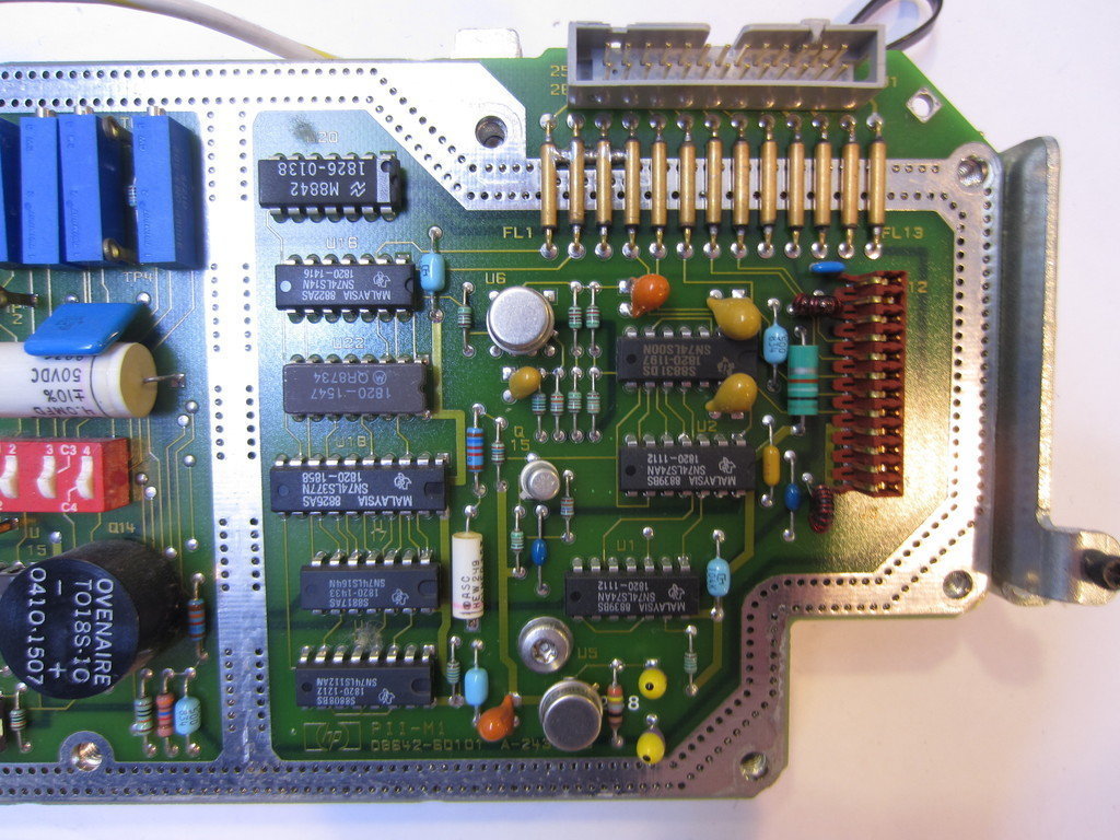
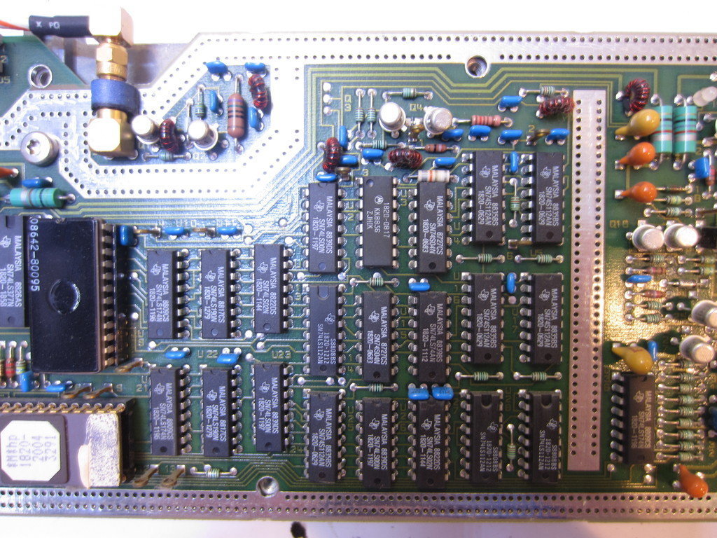
A4 Latch Module
Like A3, the layout of A4 is also pretty standard, just like how most digital boards’ layout back in the 80’s. Since the speed of these digital boards are relatively slow (under 10 MHz), propagation delays are negligible and trace routing is not super critical.
|
|
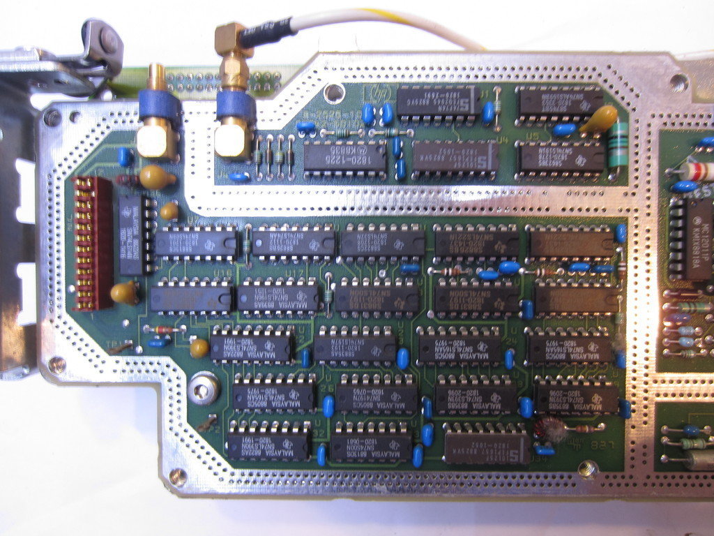
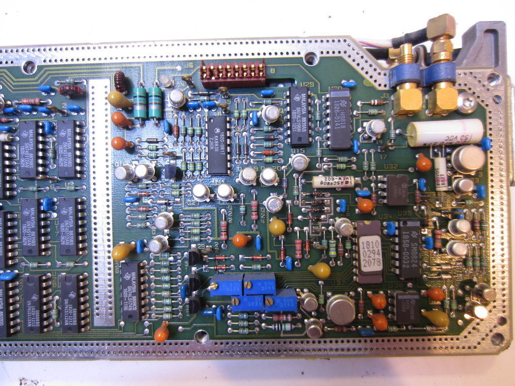
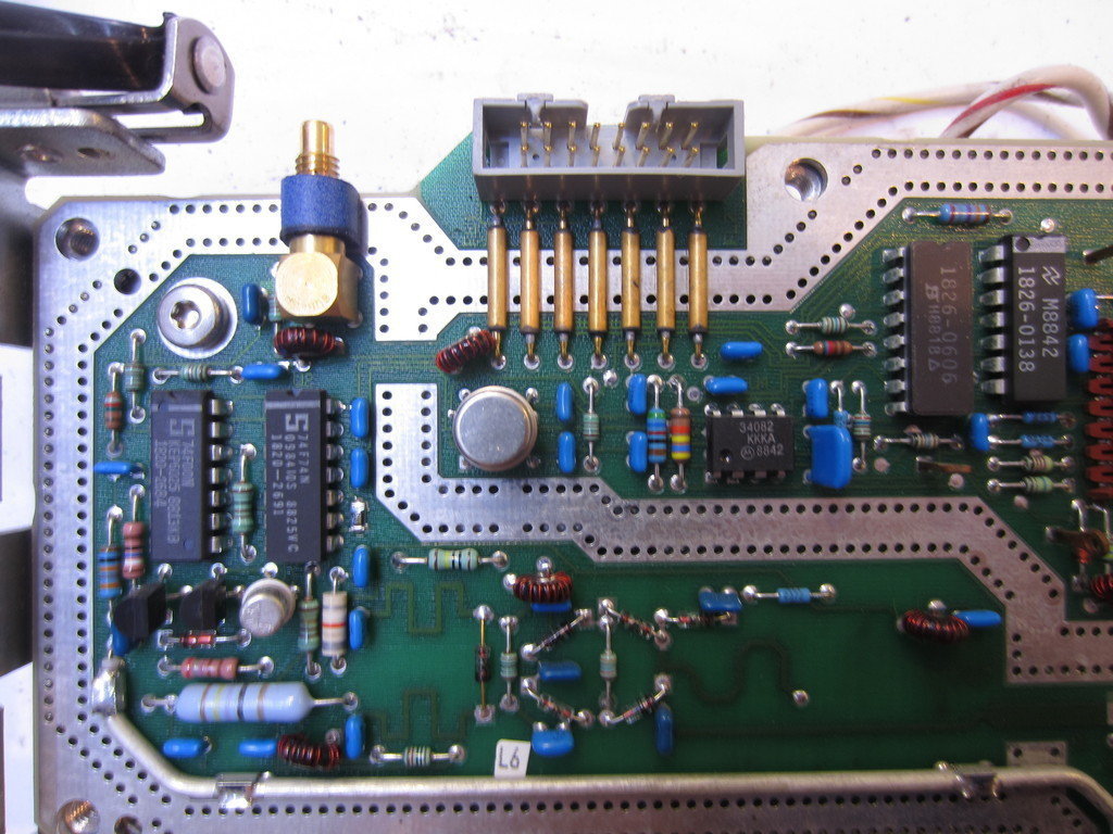
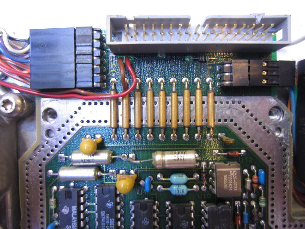
A6A1 FM Loop/Counter/Timebase Module
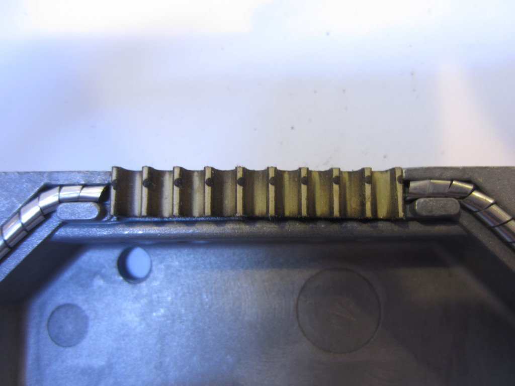
This is the first shielded module. Each side of the module is shielded via a different piece of metal enclosure. From the images below, you can clearly see the heavily via-stitched ground traces. These traces make contact with the springy contacts inside the metal cover (you can see a couple of pictures towards the end of the post) which ensure good electromagnetic shielding.
|
|
|
|
In the last picture above, you can see how signals are brought in and out of the board (via shielded lines). This technique is used throughout the high frequency sections to avoid any disturbance to the continuous ground plane.
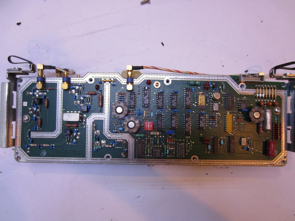
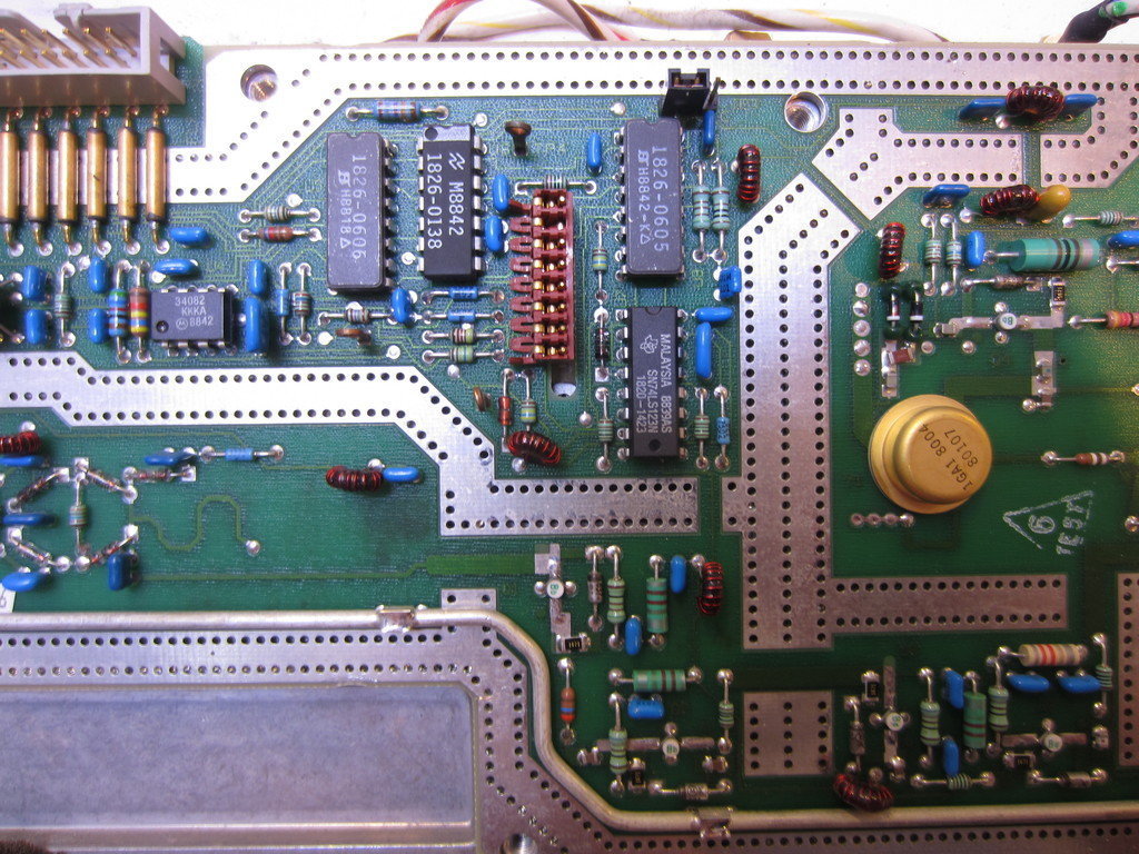
A6A2 FM Loop/Counter/Timebase Module
On this side of the A6, there are a few sections of digital circuitry.
|
|
|
|
| [adsense] |
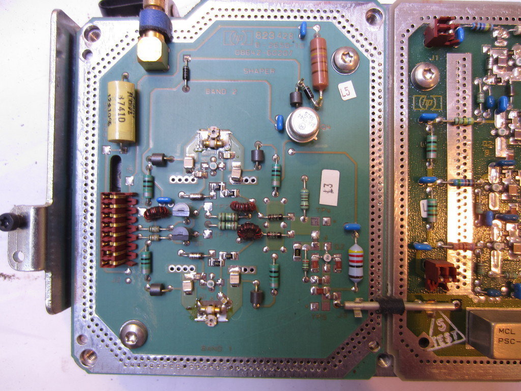
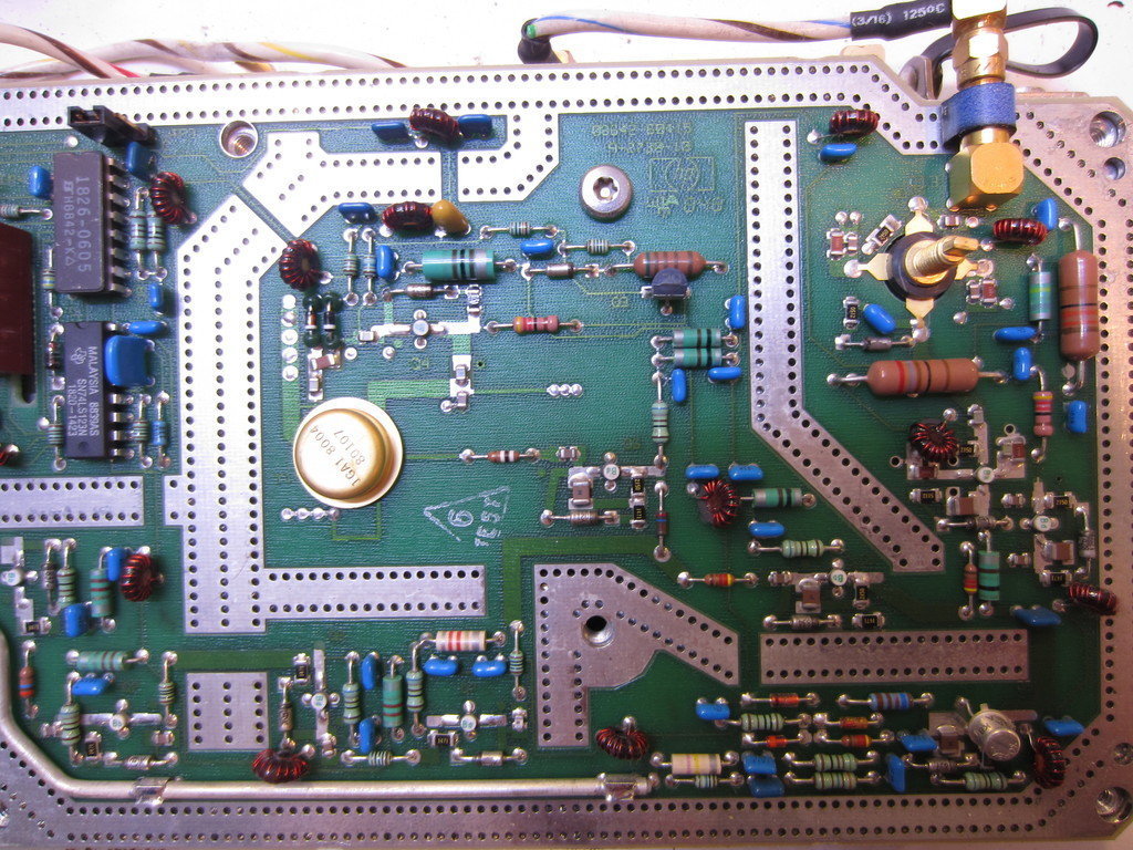
A7 SAWR Loop Module
On this board, you can see some impedance-matched traces:
|
|
|
|
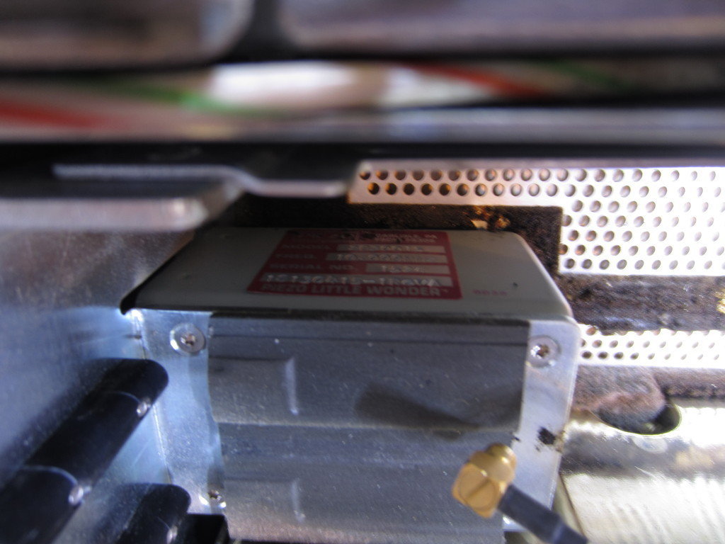
A8 High Stability Timebase (OCXO)
The high stability crystal oven lies beneath A7 and A8. In one of my previous posts, I did a teardown of the crystal oven inside the HP 5350B so I did not bother take this one out.
A9A1 IF Loop Module
On this side of the board, it is mainly the analog circuitry.
|
|
|
|
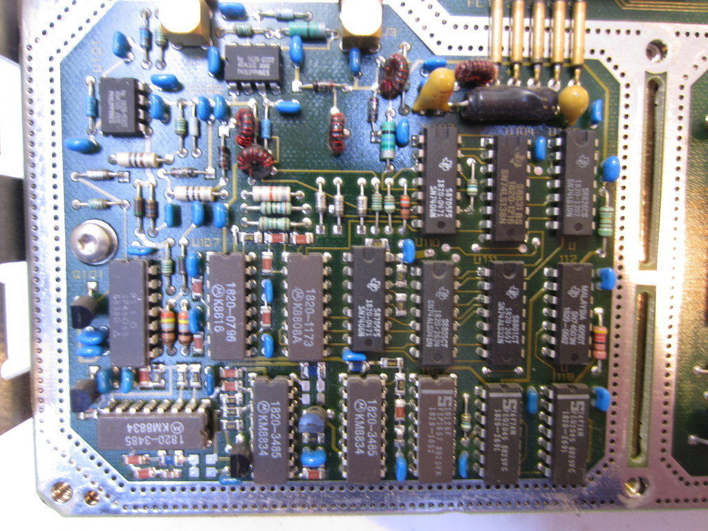
A9A2 IF Loop Module
On the A9A2 board, it is again most digital.
|
|
|
|
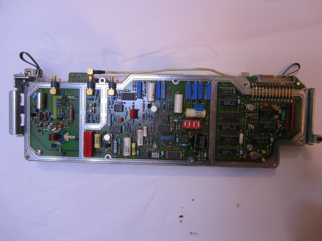
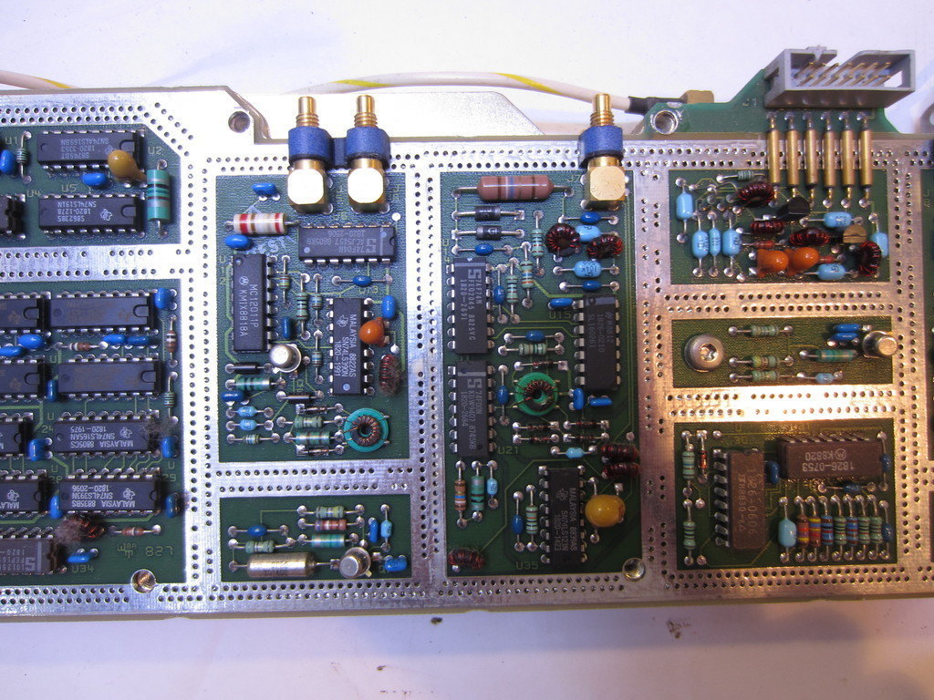
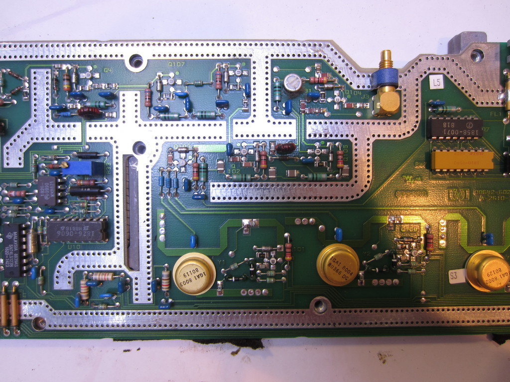
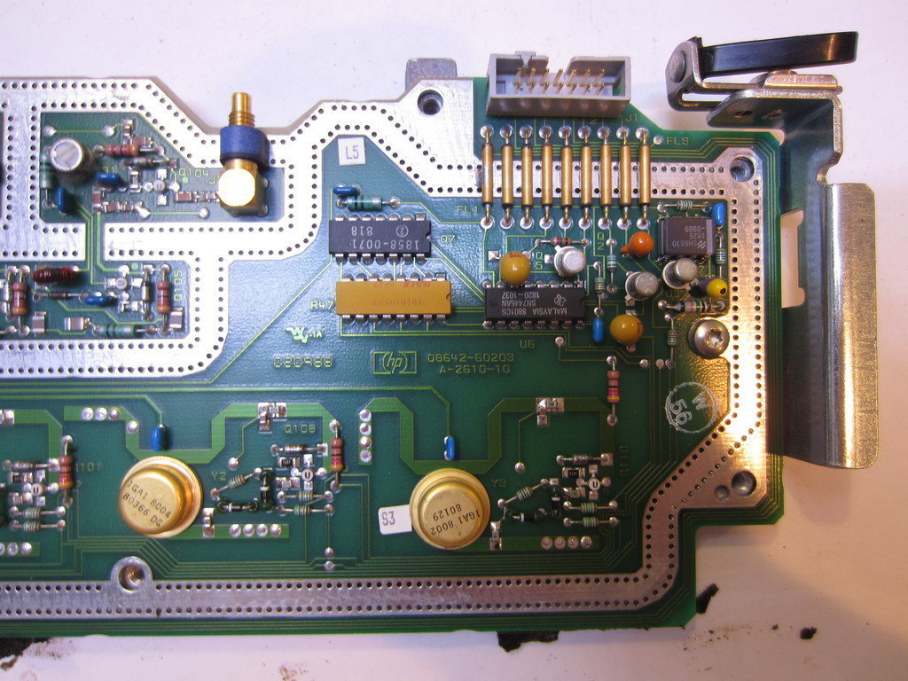
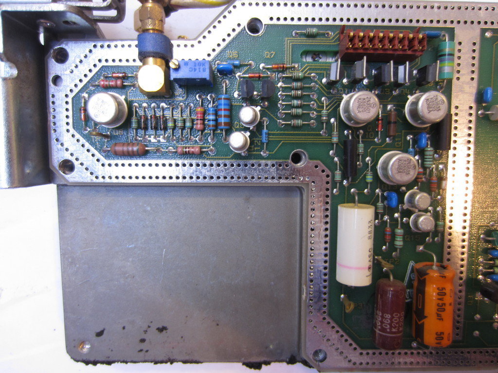
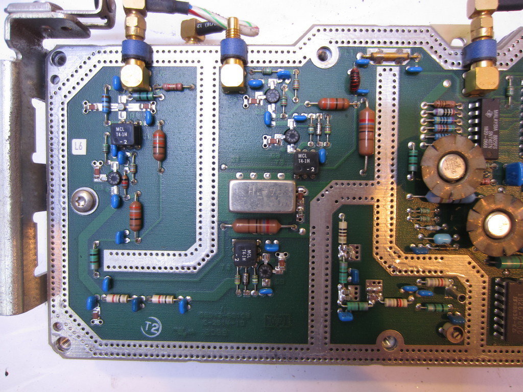
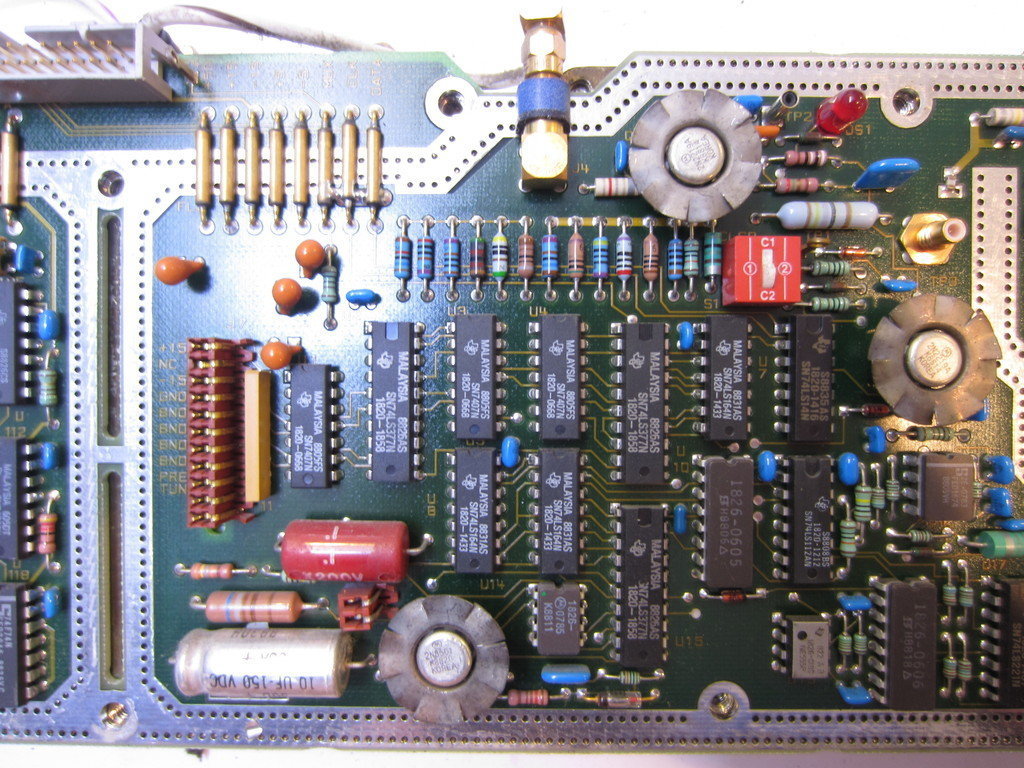
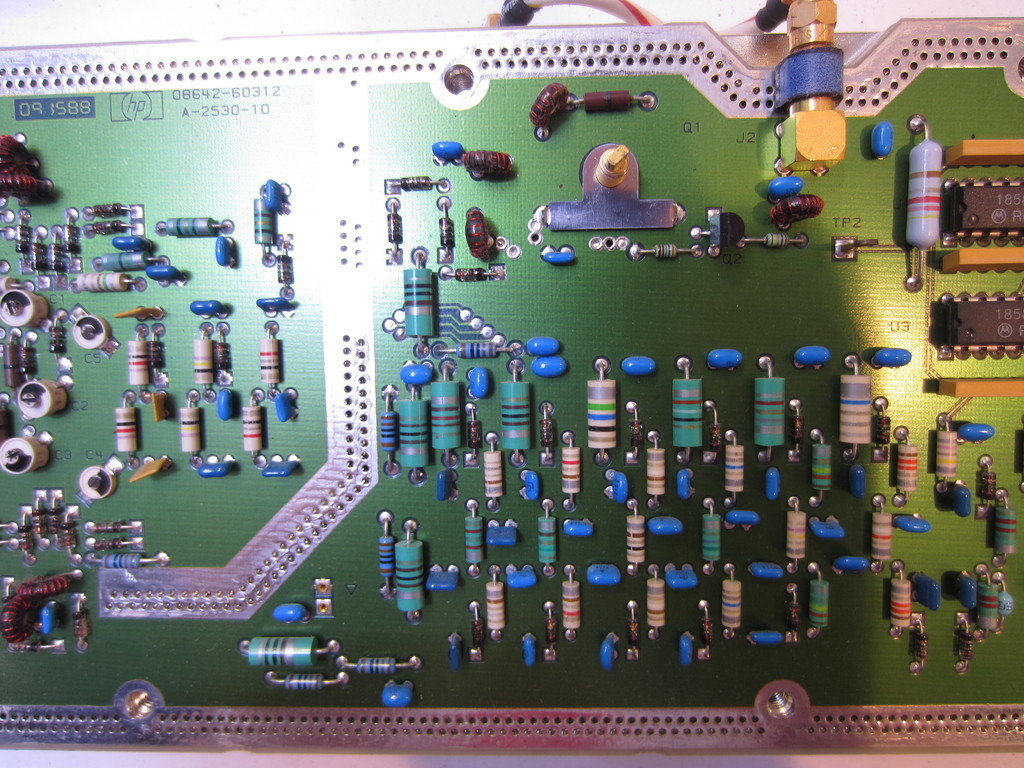
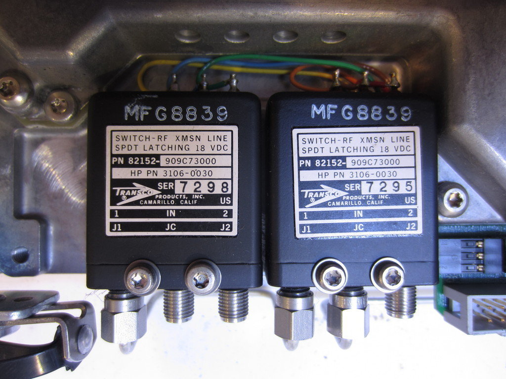
A11A1 Reference Loop Module
In this module we are going to see some RF magic. On A11A1, the left side is the RF portion and the right side is the digital portion.
|
|
|
|
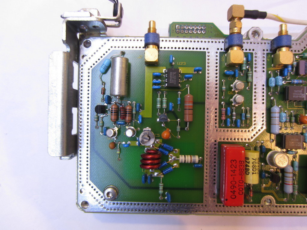
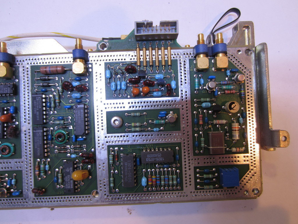
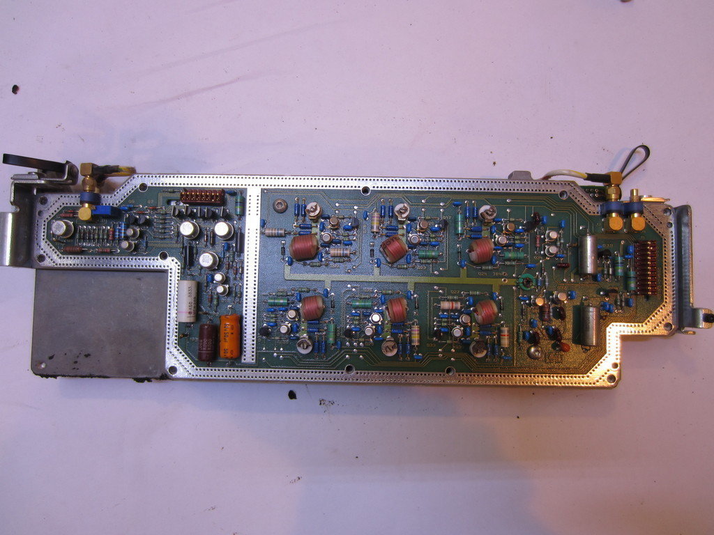
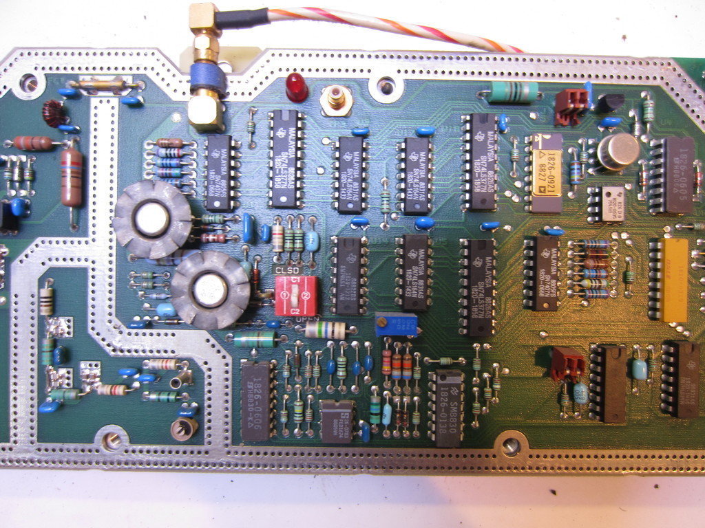
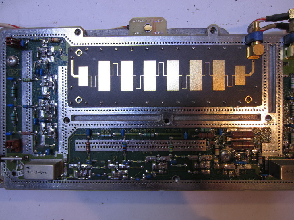
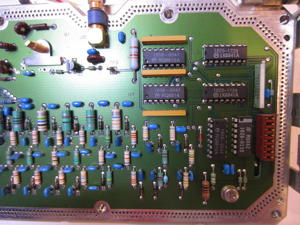
A11A2 Reference Loop Module
A11A2 is dedicated to the RF stuff. You can clearly see a few distributed element filters in the pictures below. The center filter element is custom-made onto a separate PCB (presumably different material characterized for high frequency use). And it is a critical portion of the reference loop and thus additional shielding is introduced (see the conductive foam under the shielding cover).
|
|
|
|
|
|
| [adsense] |
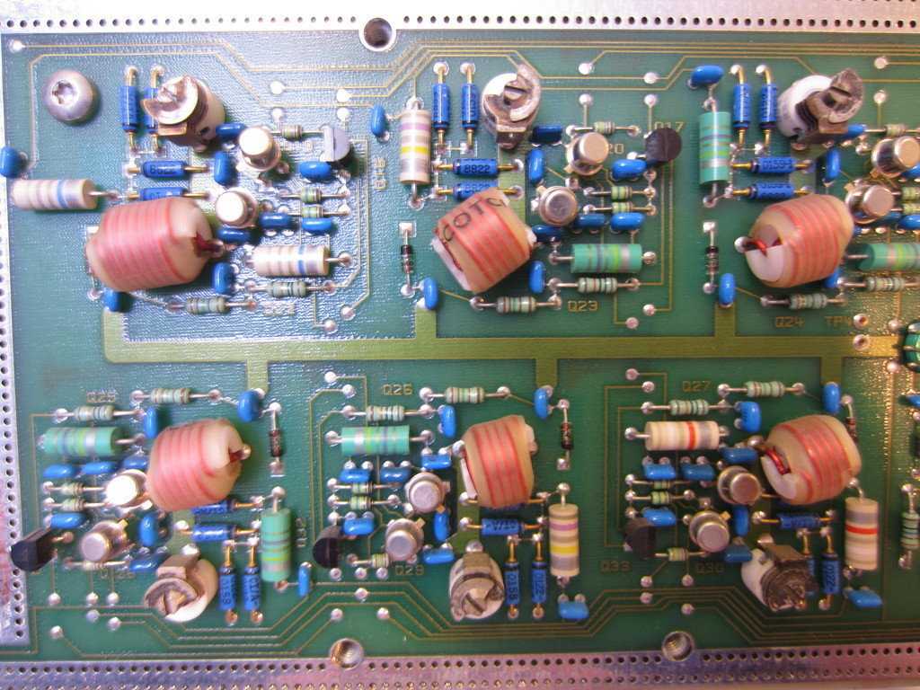
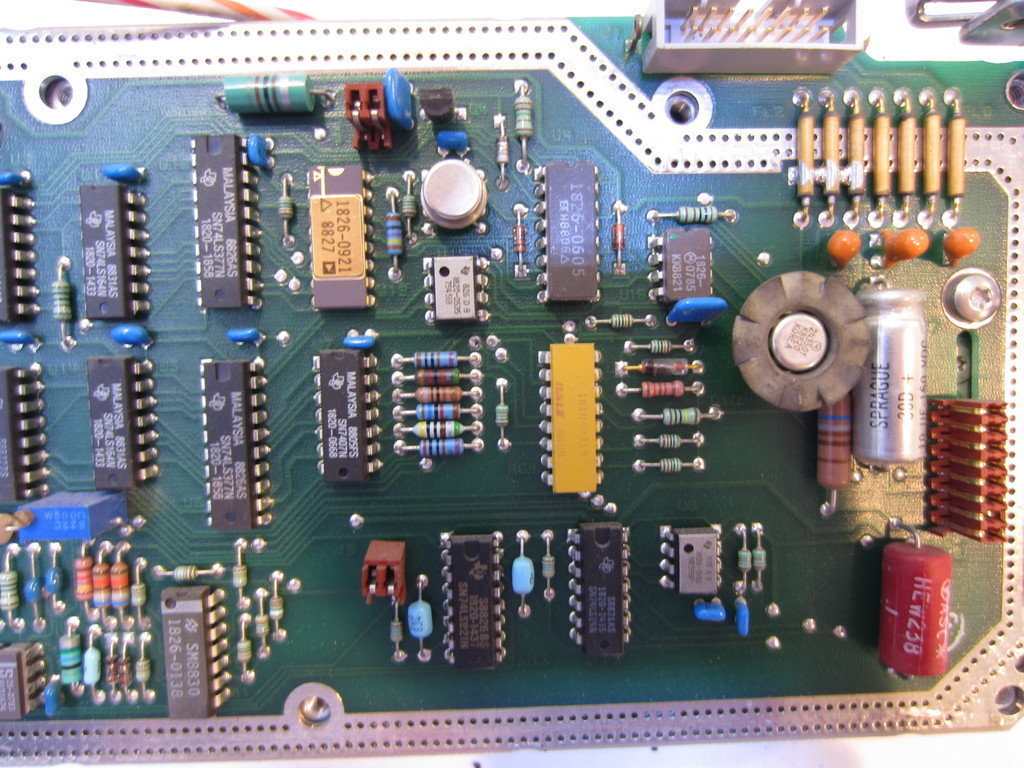
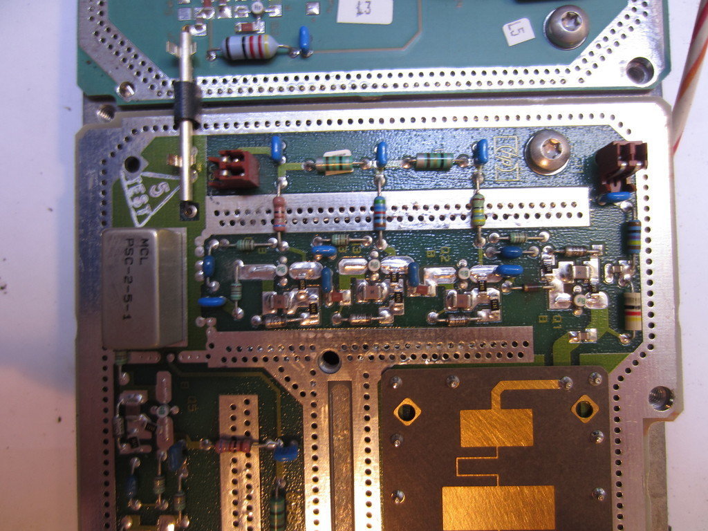
A12A1, A12A2 Sum Loop Module
More RF stuff on A12A1 and A12A2. Note how carefully the ground traces are arranged.
|
|
|
|
A12A3 Sum Loop Module
A12A3 is again mostly digital.
|
|
|
|
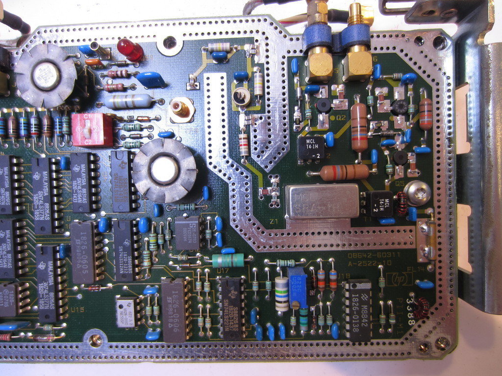
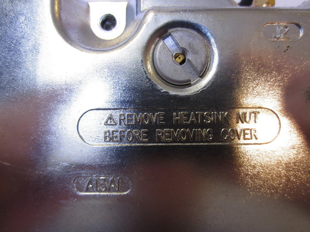
A13A1 Output Filter/ALC Module
You will need to be careful when opening up the shielding case on both A13 and A14 modules as they have heatsink nuts screwed on them. In order to open the case these nuts must first be removed. On A13, the heatsink nut is attached to the RF power amplifier module on the A13A2 board.
Note that ground plane is floodfilled on A13A1.
|
|
|
|
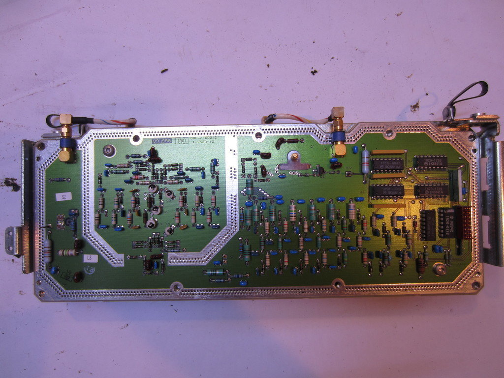
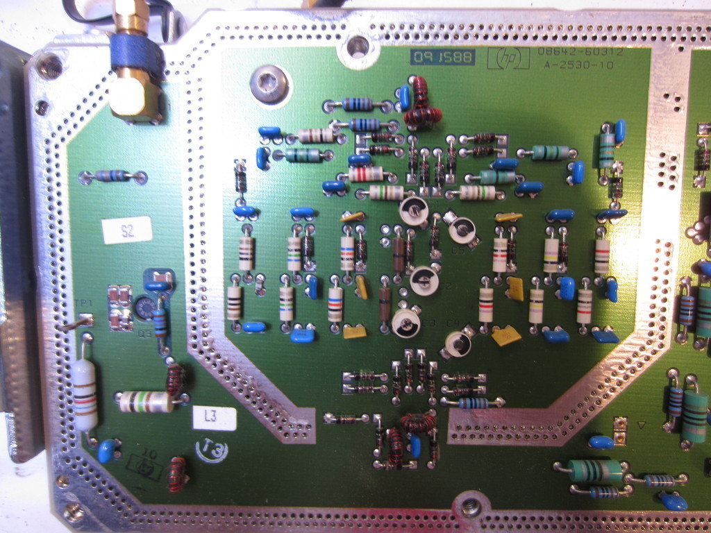
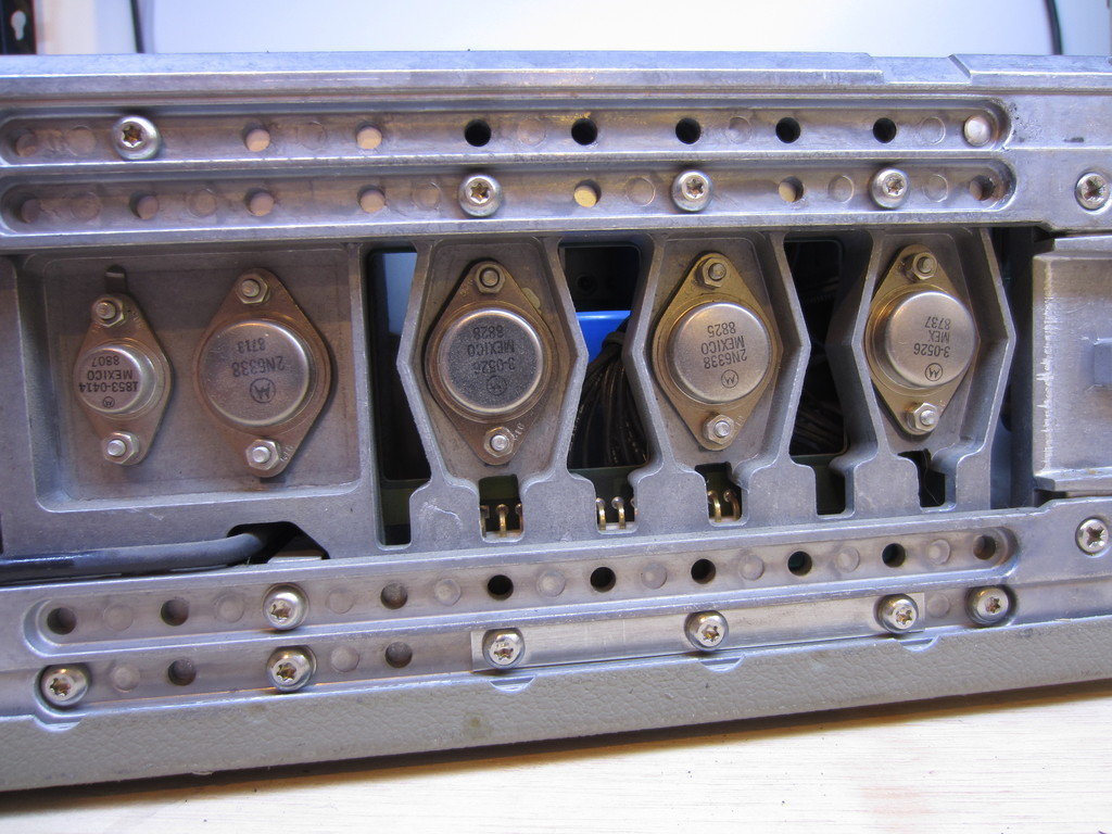
A13A2 Output Filter/ALC Module
You can see the RF module in the center. In the last picture, you can see some impedance matching traces. Again, signals are routed into this section via feedthrough capacitors above the ground traces.
|
|
|
|
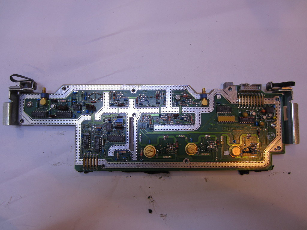
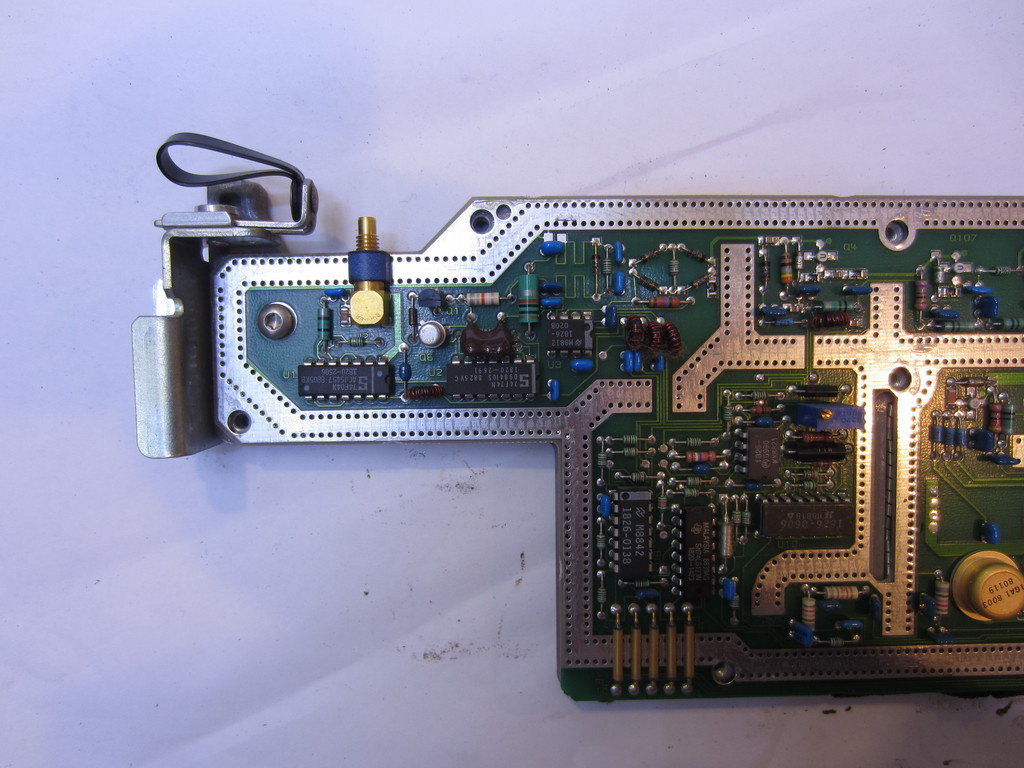
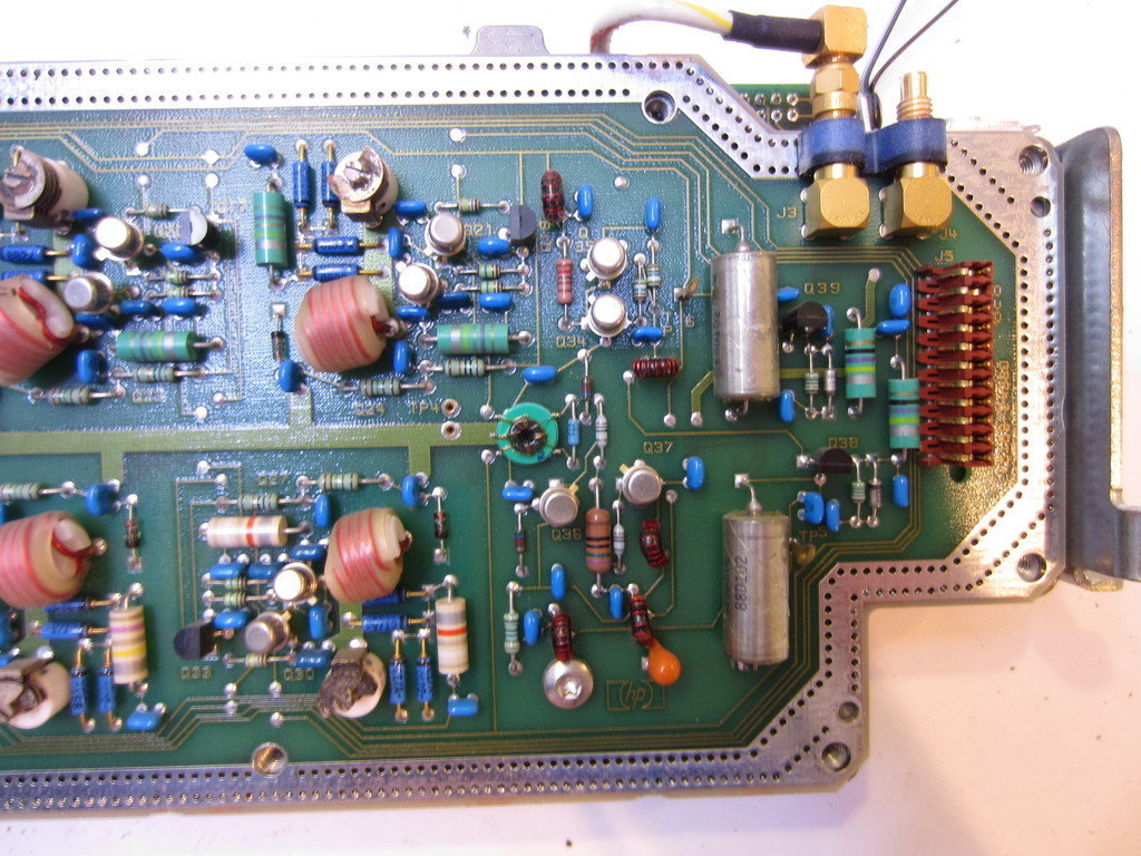
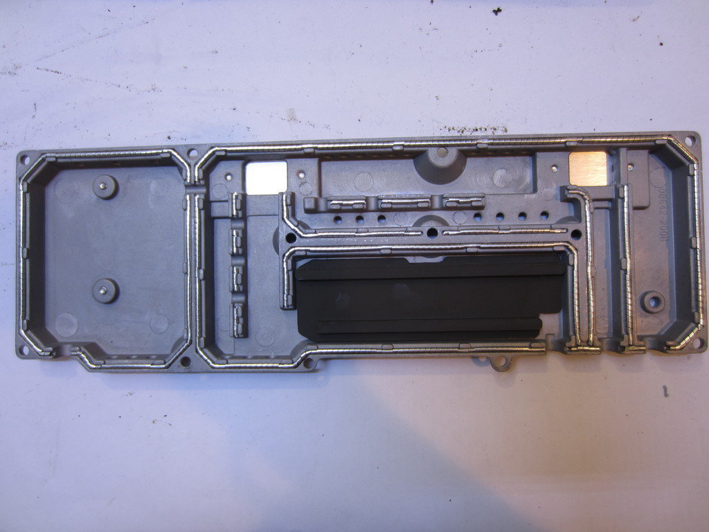
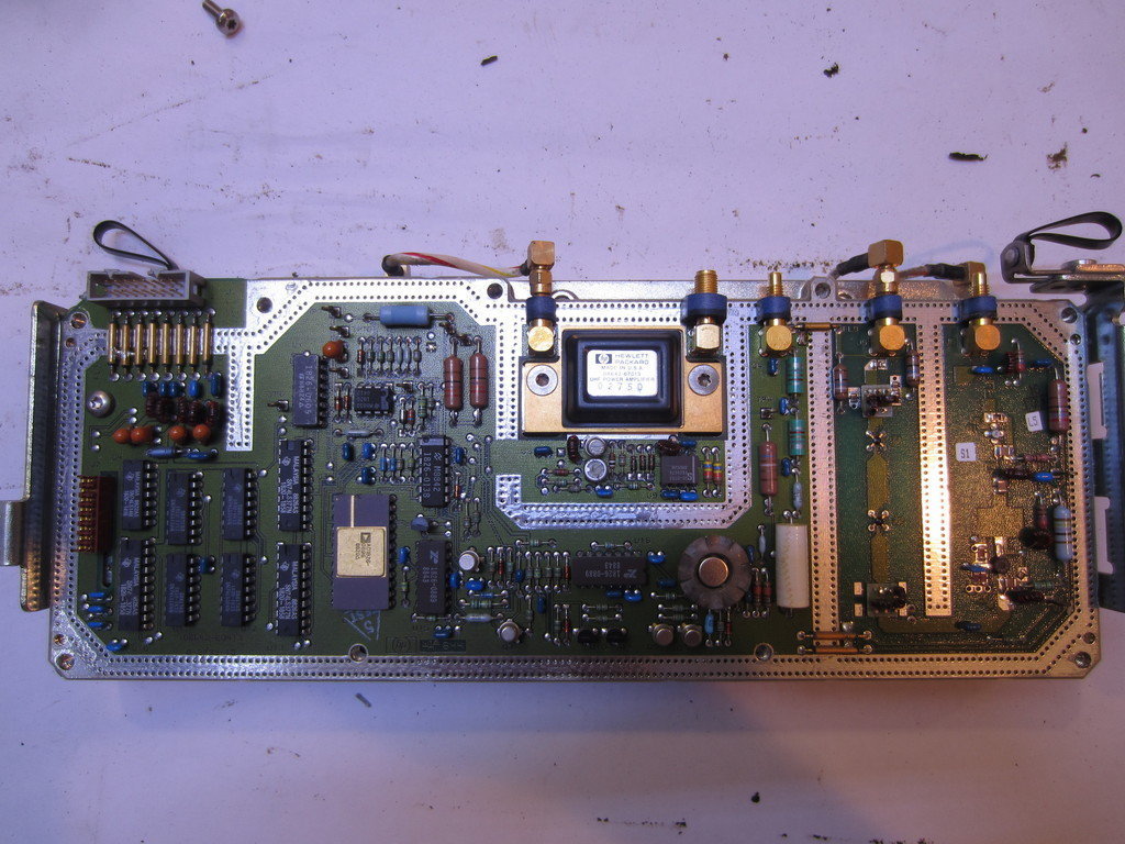
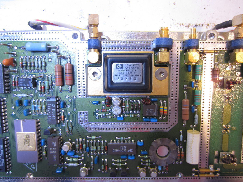
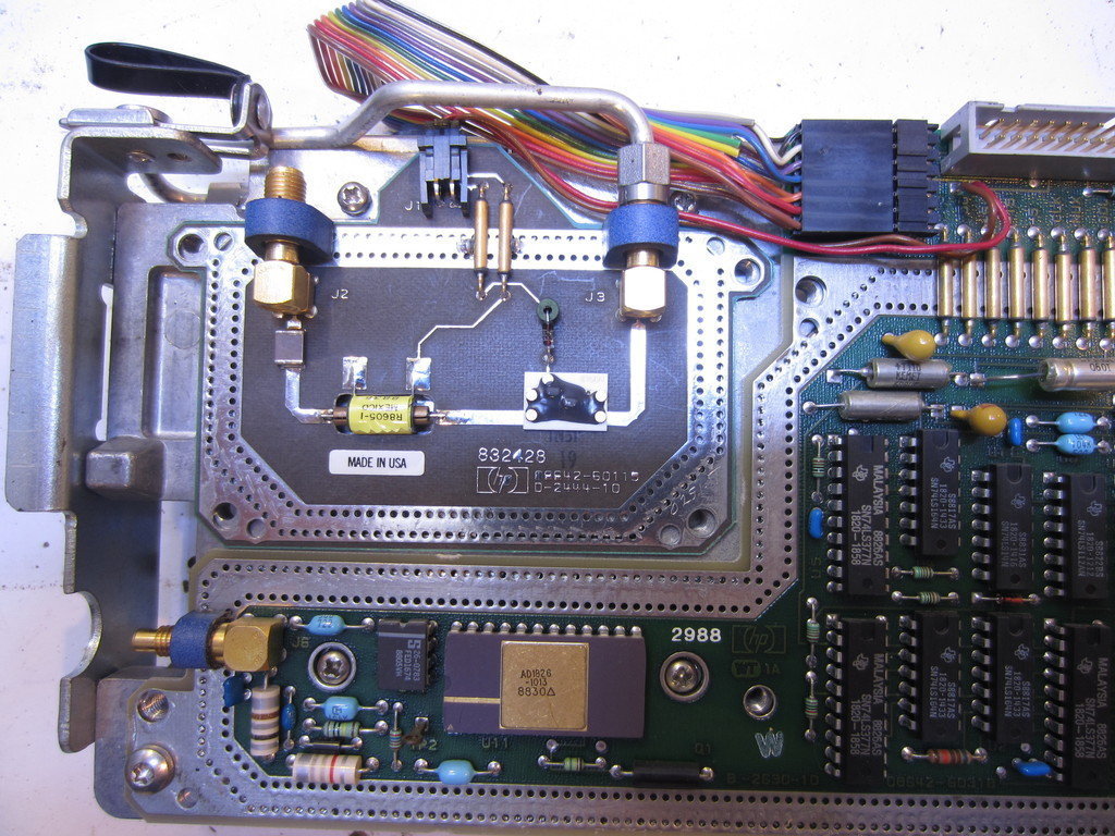
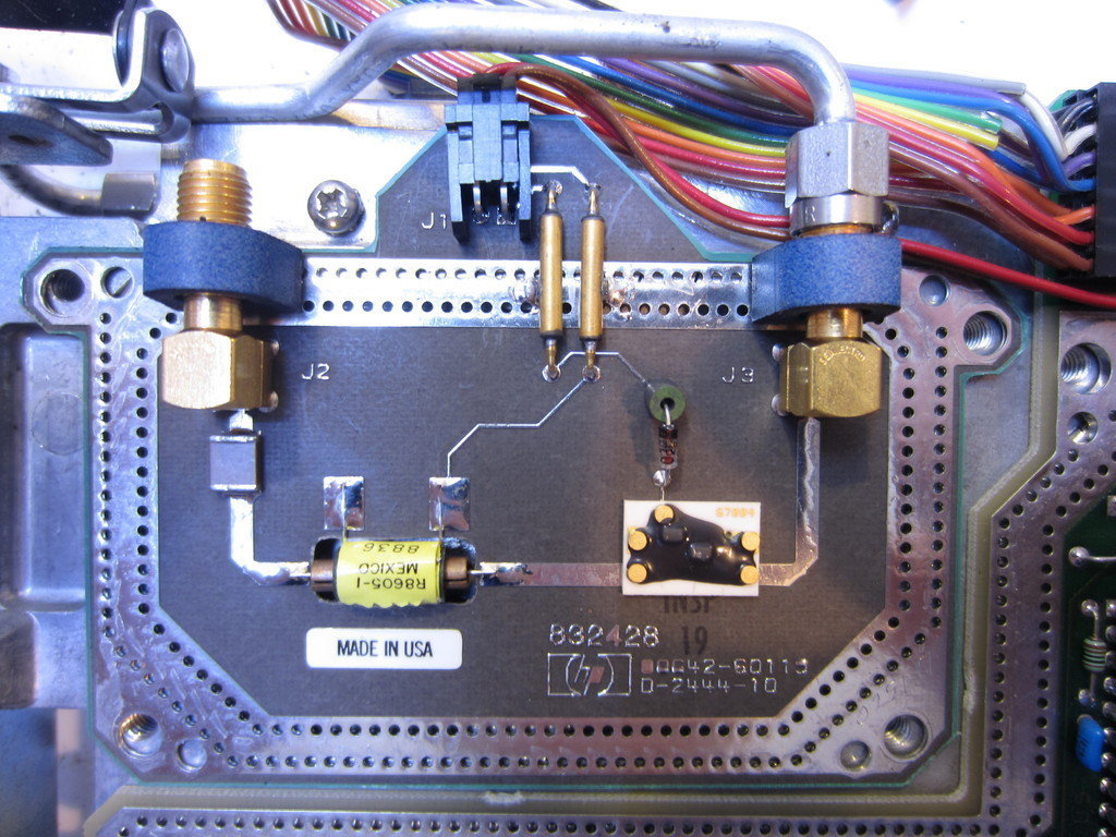
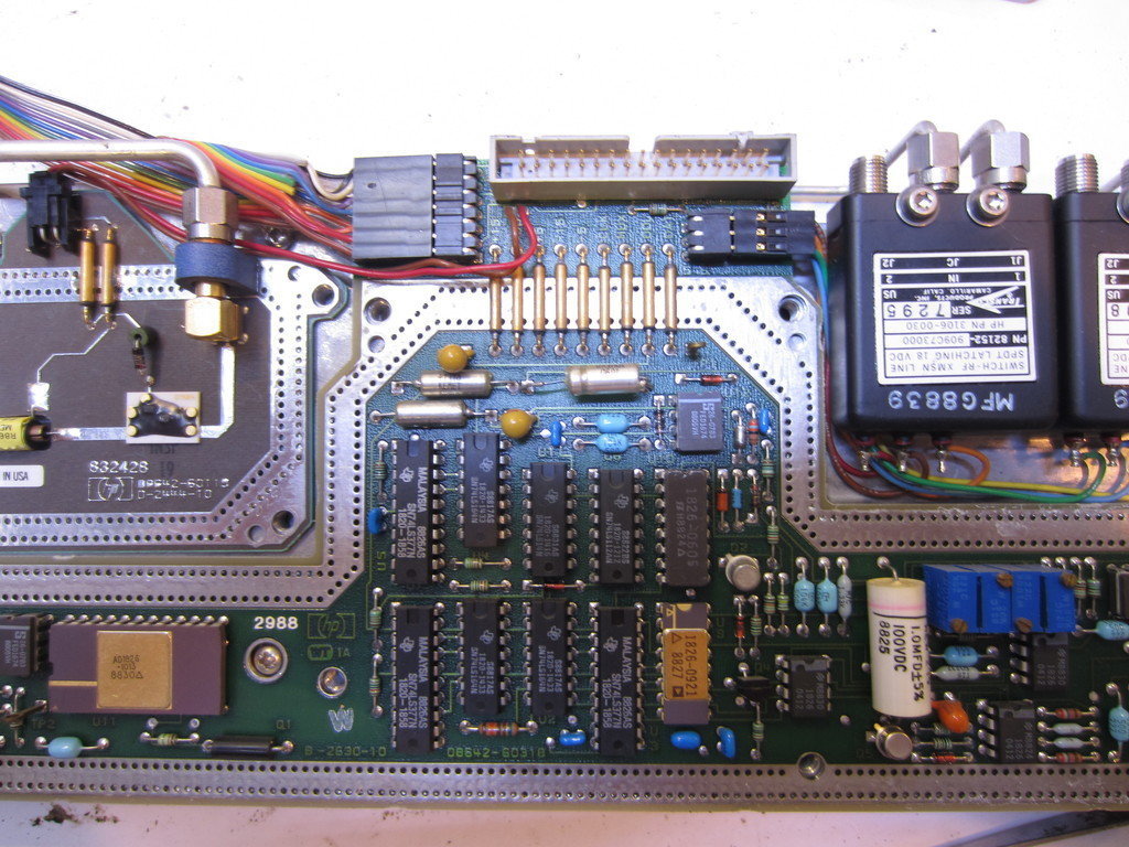
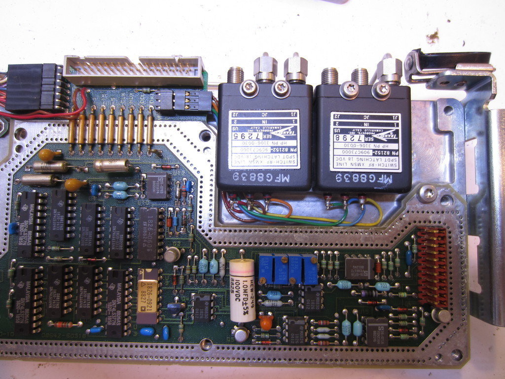
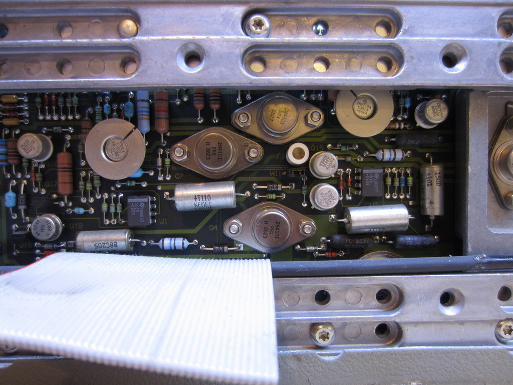
A14A1 Heterodyne Module
The first picture is the full view of the Heterodyne module. The assembly with the SMA connectors is the HET switching unit. Again, the circuit sections are separated by via-stitched ground. The heatsink nut is connected to one of the RF transistors.
|
|
|
|
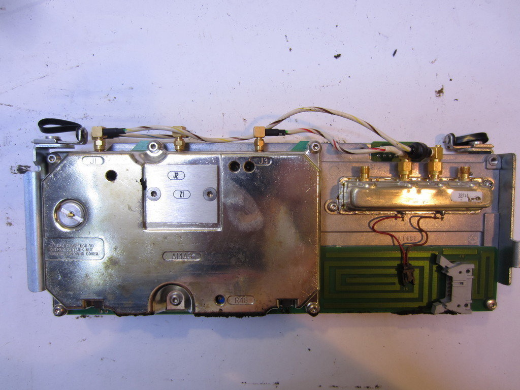
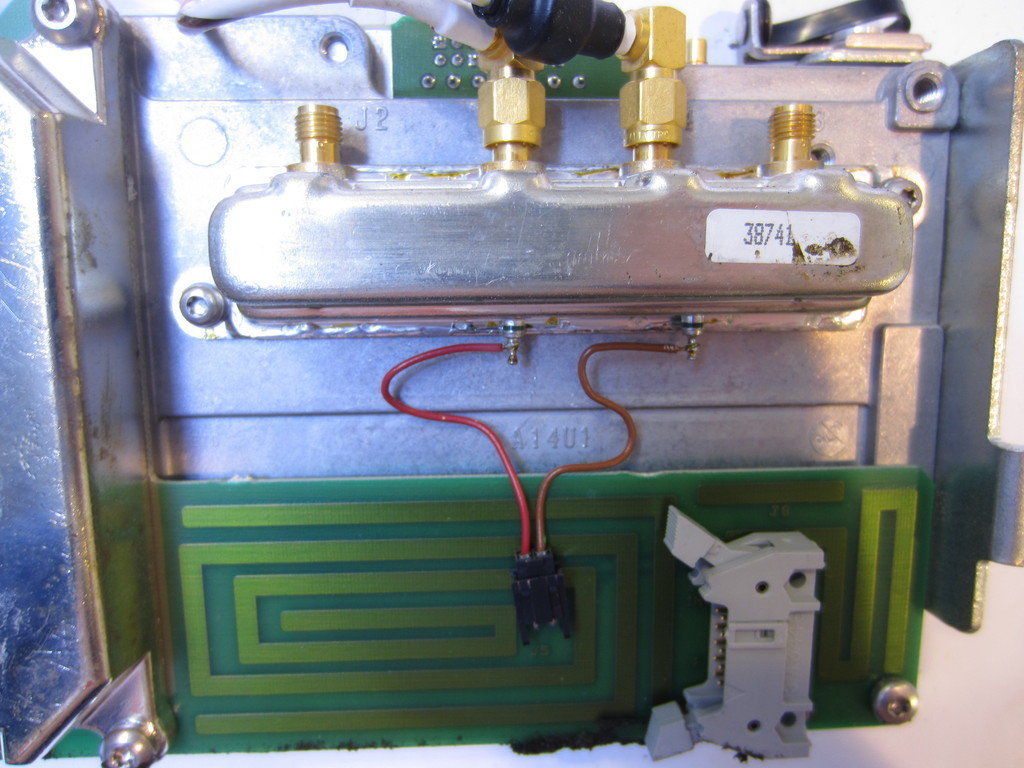
Here is a picture of the RF shielding cover on the A14A1 side.
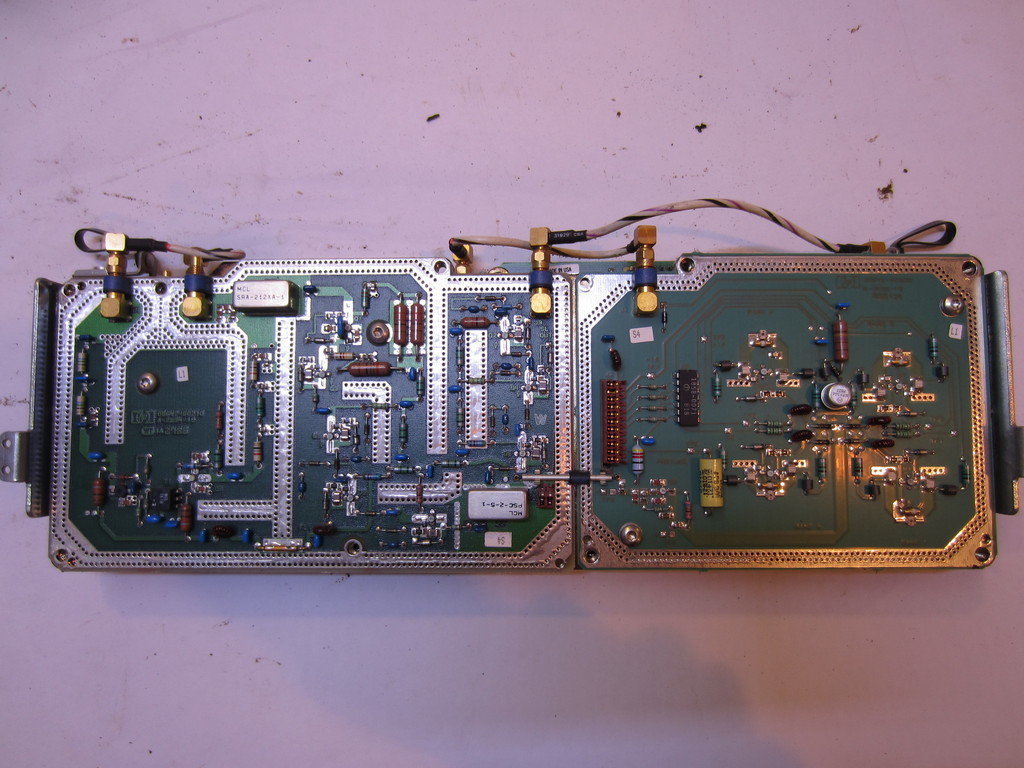
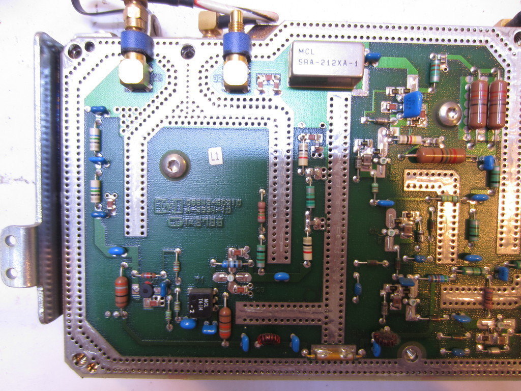
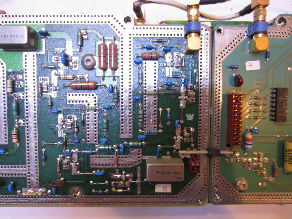
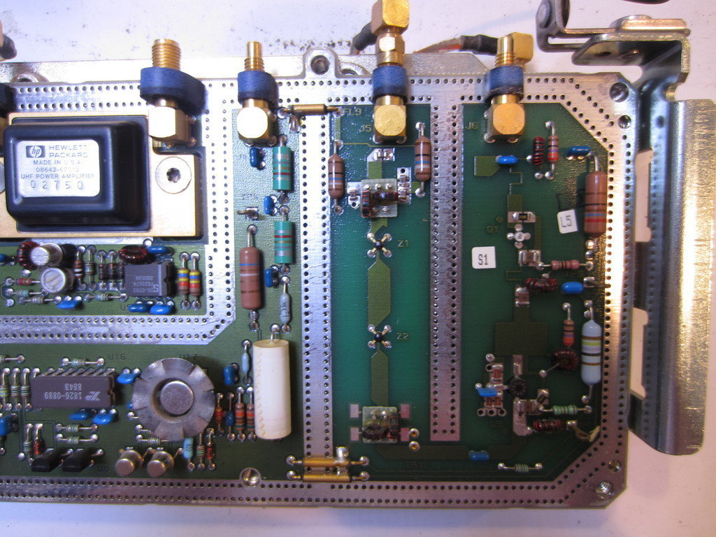
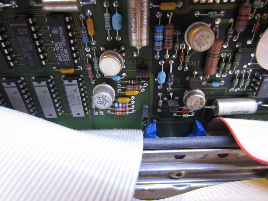
A14A2 Heterodyne Module
|
|
|
|
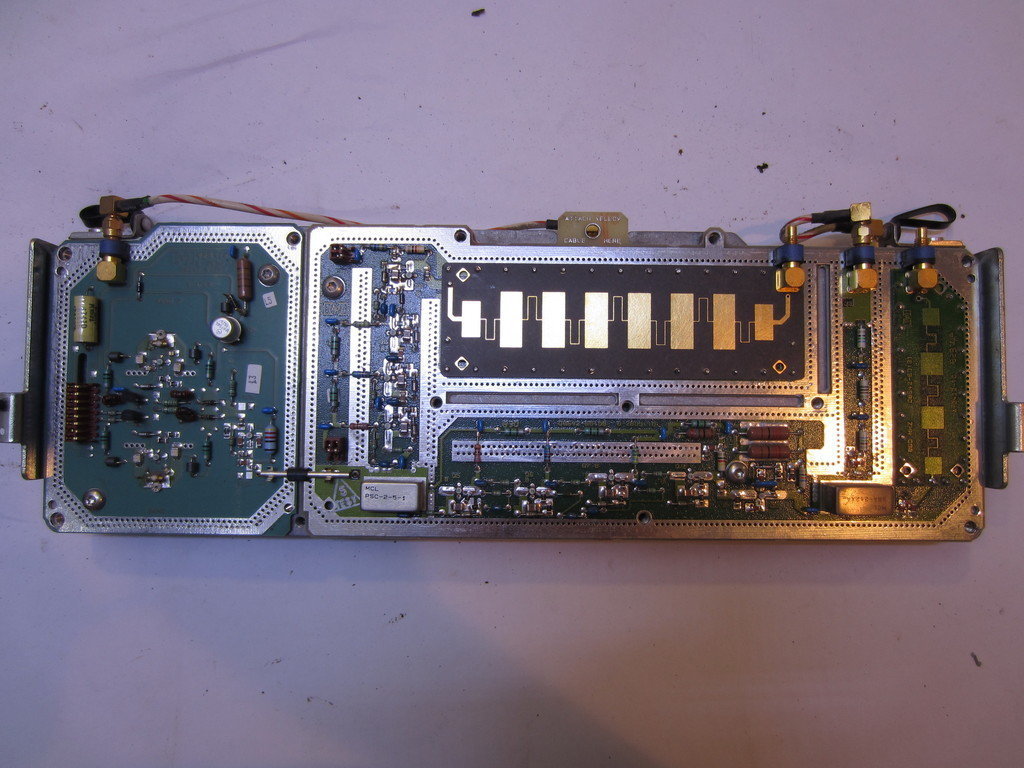
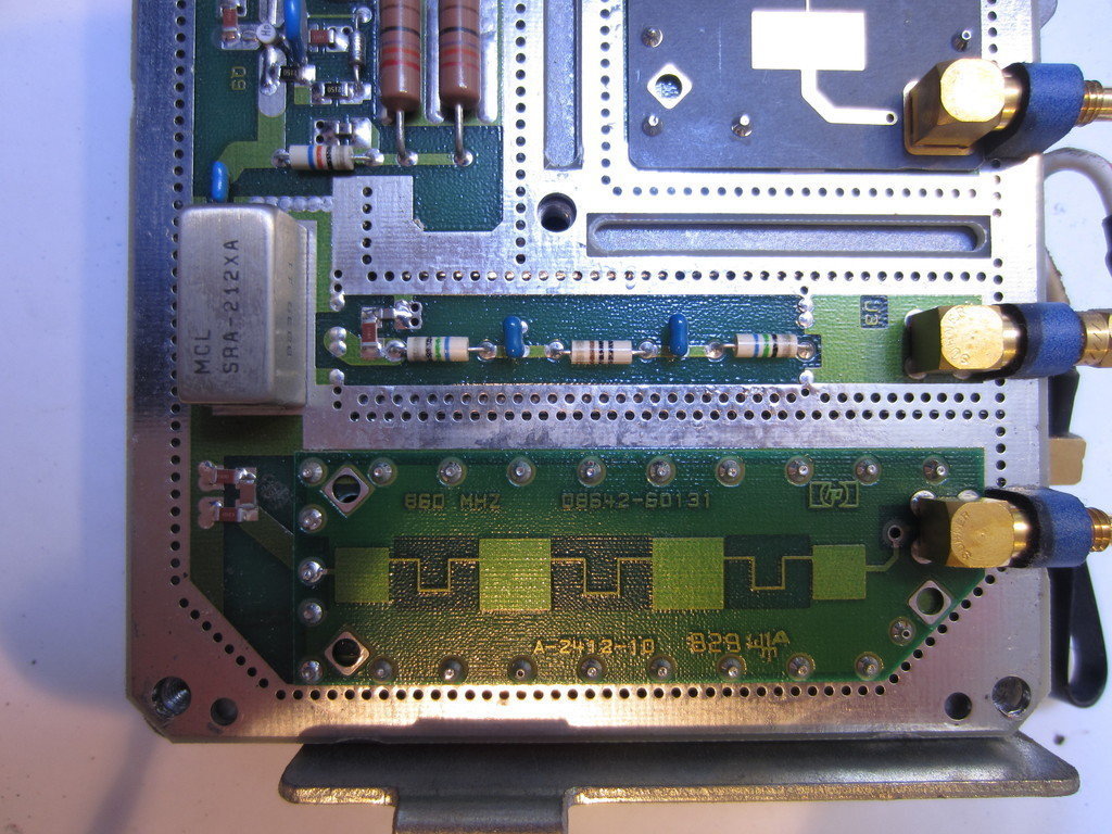
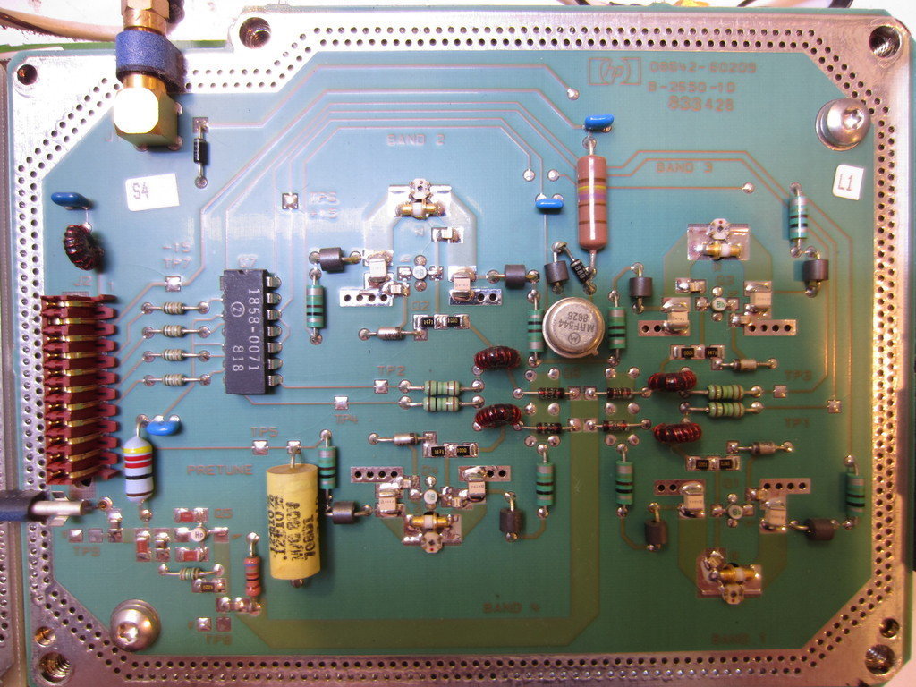
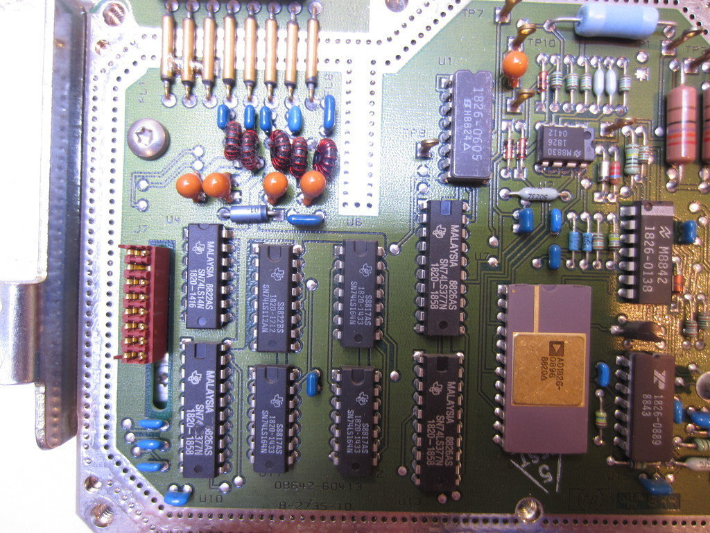
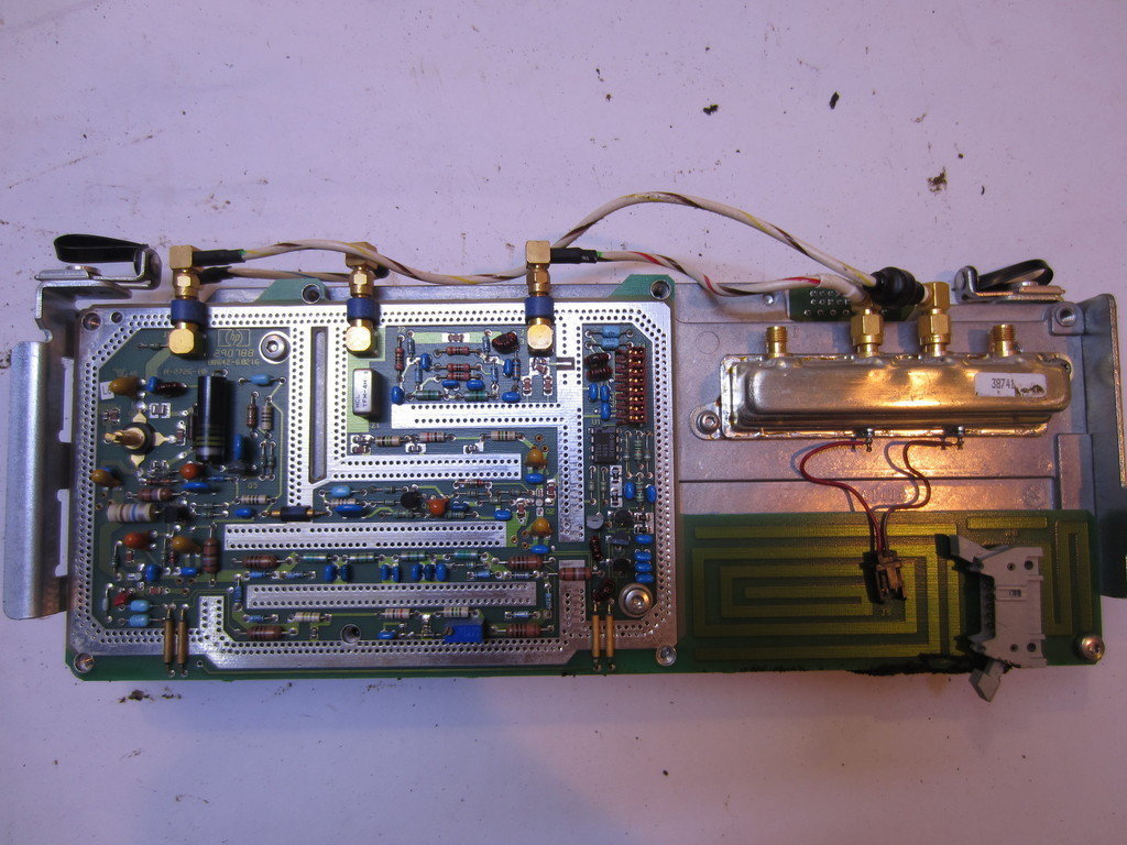
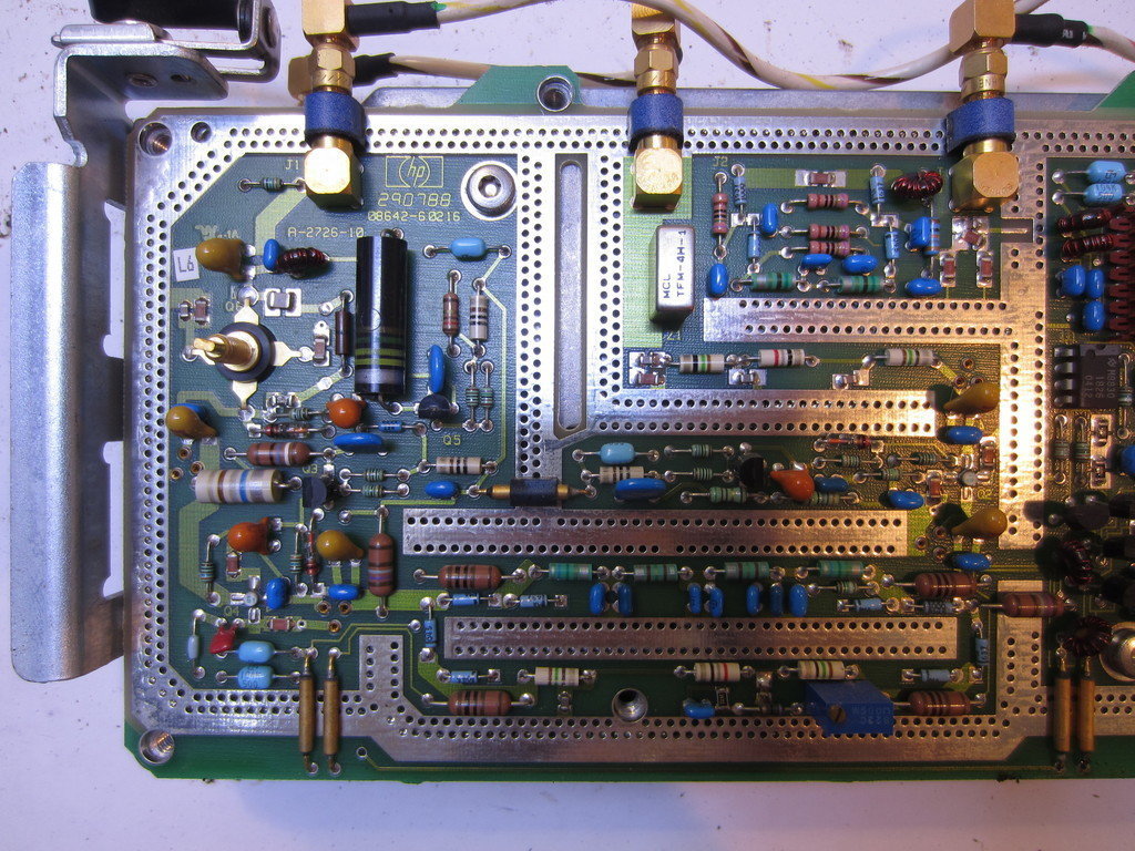
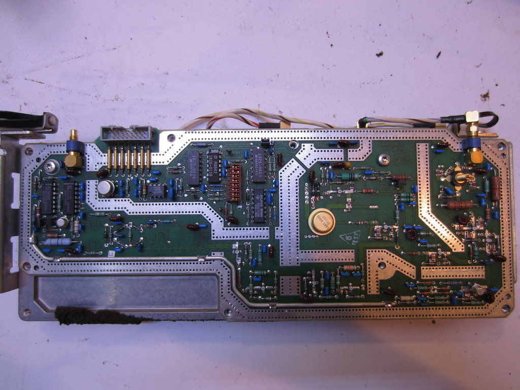
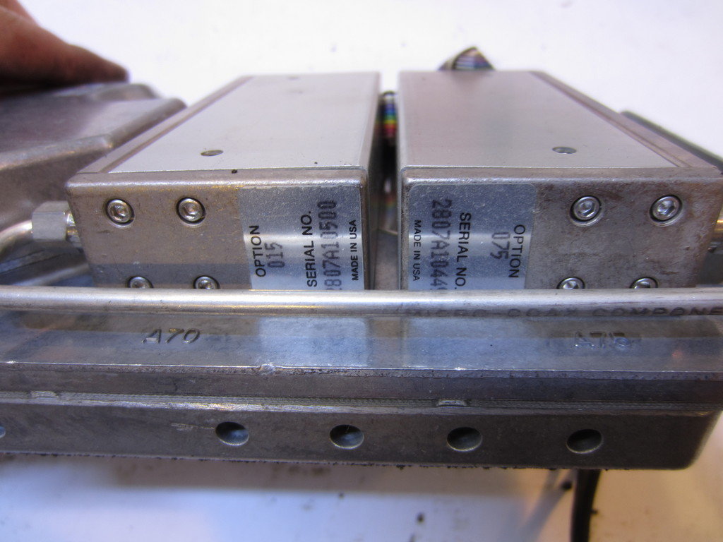
A19 Doubler/Attenuator
A19 is the only hardware difference between HP 8642A and HP 8642B. On the A model, this module is replaced with the A16 attenuator module. Of course, the firmware between these two models are different as well.
|
|
|
|
|
|
|
|
|
|
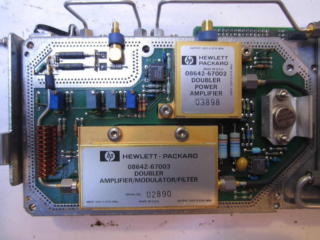
Most of the RF circuitry are handled by the doubler power amplifier, doubler amplifier/modulator and filter circuit modules.
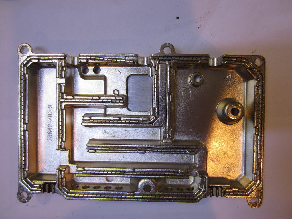
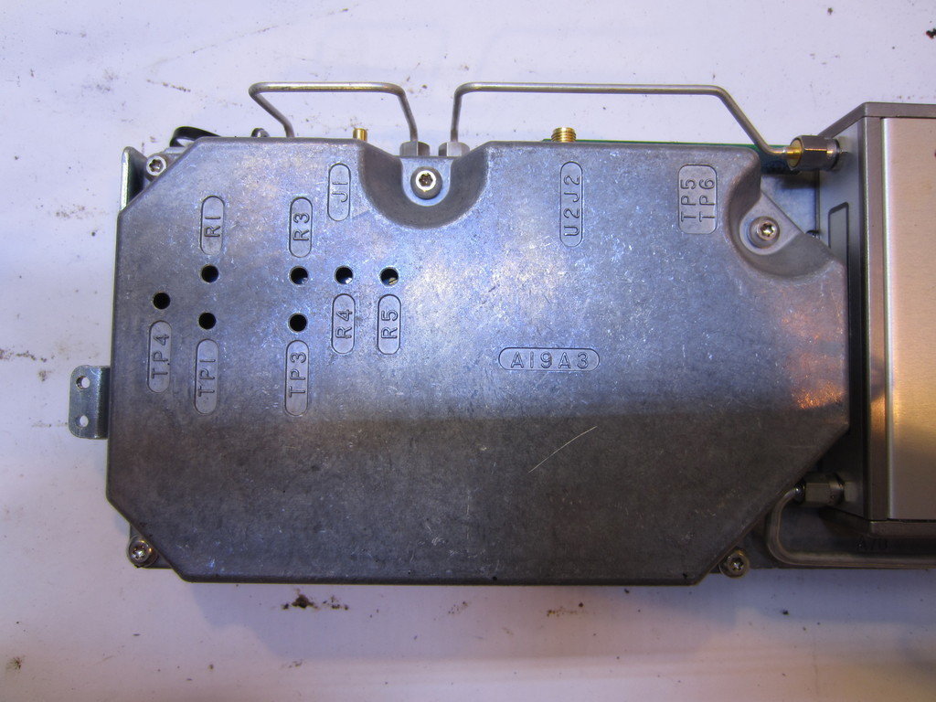
Here is a close up showing how signals are brought into the ground-plane-enclosed area via feedthrough capacitors. The outside of these capacitors is grounded and sealed off via the matching grooves on the shielding cover.
|
|
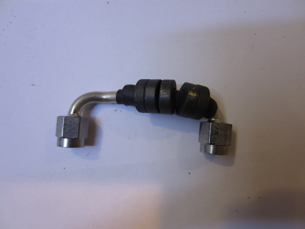
There are a lot of rigid coaxes connecting A14 and A19 (see pictures in my previous post), one of the rigid coax is especially interesting. It passes through quite a few ferrite beads for the maximum noise reduction.
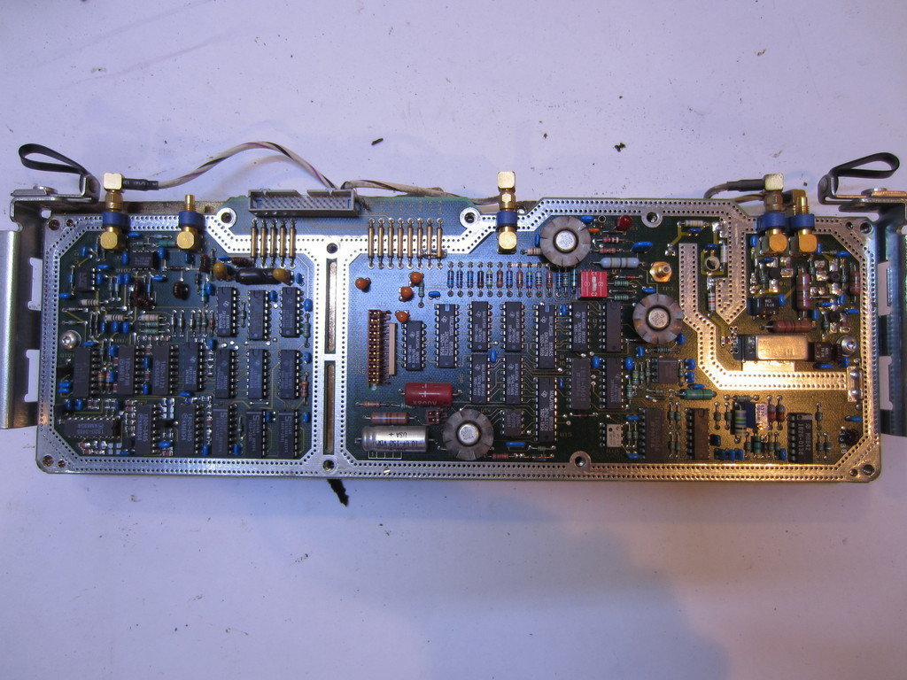
A17 Power Supply
The regulator portion of the the power supply circuitry is located on the right side of the unit and can be accessed by removing the right panel.
|
|

