Today at a time when digital storage oscilloscopes (DSO) are almost ubiquitous, analog scopes like Tektronix 2465 remain popular among many electronics hobbyists, especially among amateur radio operators who routinely work with high frequency circuits. I got my 2465 from ValueTronics. For those who haven’t heard about them, I would recommend you check them out as they have a large selection of used test equipment at reasonable prices.
When Tektronix first introduced this oscilloscope back in 1984, it cost a fortune. Now thirty years later, anyone who wants to own a fine analog scope can get his hands on one. At a price of several hundred dollars, very few oscilloscopes (used or new, including modern DSOs) can match its 300 MHz bandwidth and advanced triggering capabilities.
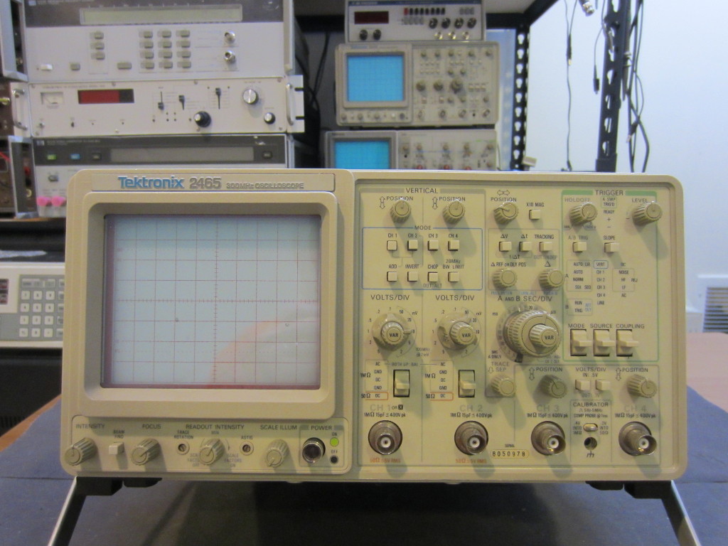
In the picture below, you can see the 4-channel 300 MHz Tektronix 2465 in the foreground. The oscilloscope on the top in the background is my 150 MHz Tektronix 2445, which looks almost identical to the 2465 except that its horizontal sweep rate goes from 1s/div to 10ns/div instead of the 0.5s/div to 5n/div range on the 2465.
The 2465 has four independent channels. Chanel one and channel two have independent vertical deflections range from 2mV/div to 5V/div in 11 steps via processor-controlled attenuator networks. The inputs into these two channels can be configured as either AC coupled or DC coupled with an input impedance of 1Meg or 50 Ohm (for DC coupling only). The 50 Ohm input impedance option is extremely useful when measuring various RF circuits as proper termination is usually required.
Channel three and channel four use fixed attenuators with two gain settings. These inputs are DC coupled with 1 Meg input impedance only.
An instrument pouch can be mounted on top of the scope for the convenient storage of manuals and probes alike. This particular unit did not come with the pouch, but you can see the three mounting holes where the pouch plate would be placed.
|
|
The rear cover is secured on by four screws around the edges on each of the protruding plastic stand and two in the middle towards the upper and lower edges of the rear panel. After removing the back cover the main instrument cover can then be slid off from the back.
The fan in this Tektronix 2465 runs at low RPM most of the time and is extremely quiet. Its speed is determined by a temperature controlled fan controller. The cover on top of the fan helps improving the air intake efficiency as the vents on the back cover are located on the sides. In some units, the fans used was are squirrel cage type and those fans were equally quite.
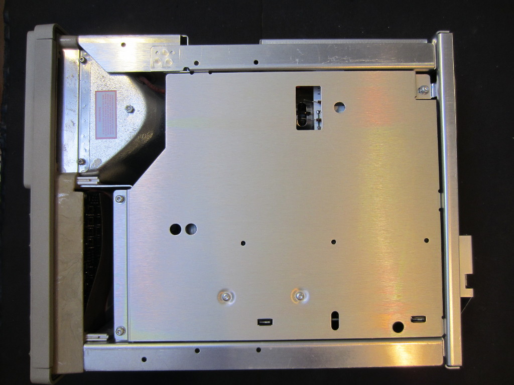
Here is a picture showing the top aluminum plate after the case has been removed. This cover is more for safety considerations than for shielding purposes as dangerous voltages exist in the the switching power supply and the CRT circuitry underneath.
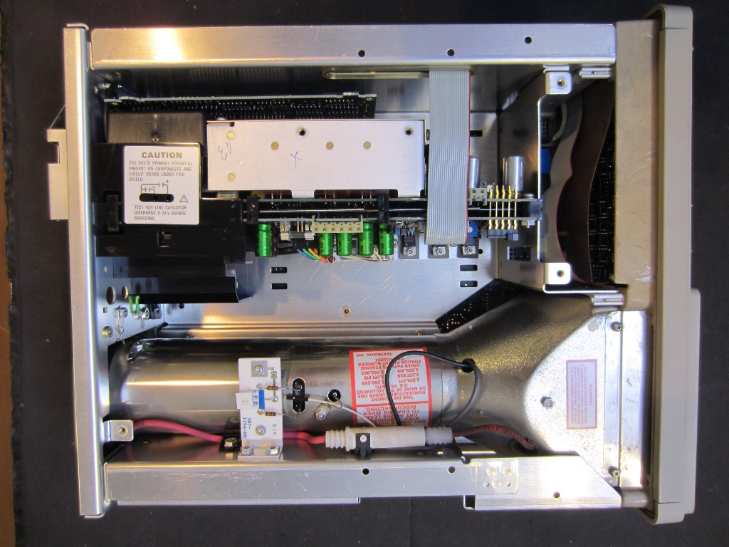
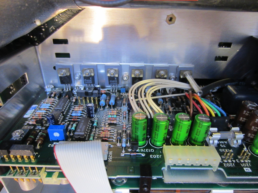
The picture below shows the interior of the scope with the top aluminum plate removed. Towards the middle you can see the A2 regulator board and the A3 inverter board. Together, these two boards provides all the regulated low voltage rails used throughout the system.
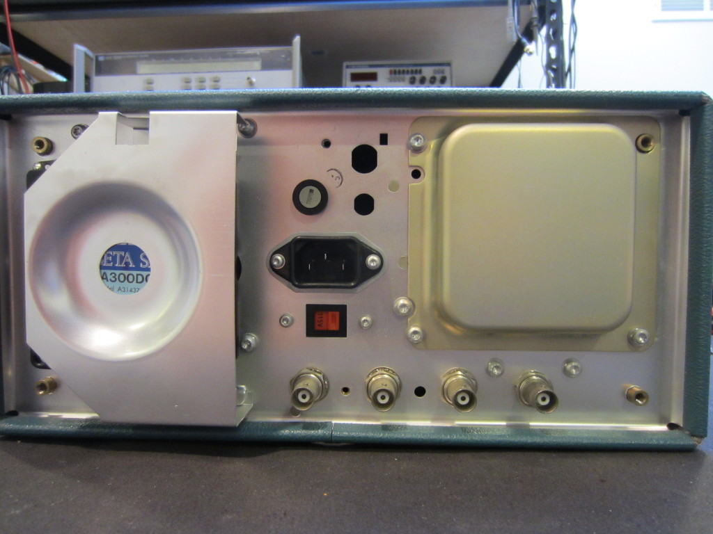
A switching power supply is used in this scope so no bulky mains transformer is present. The switching power supply circuitry is located under the aluminum cover towards the top part of the chassis.
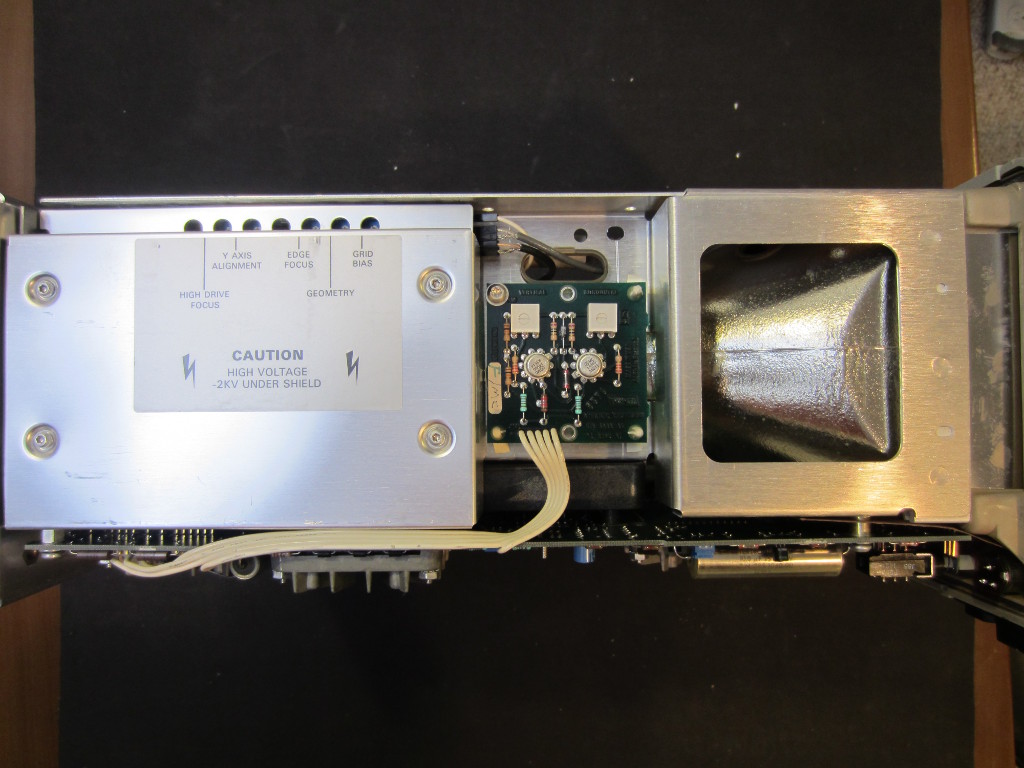
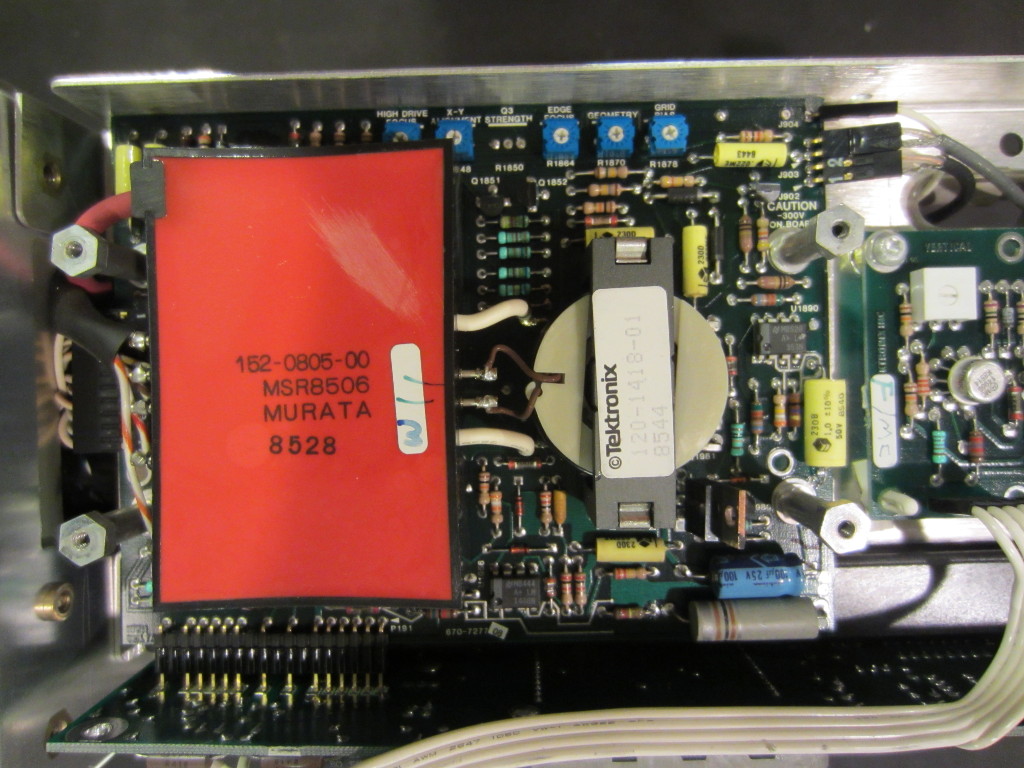
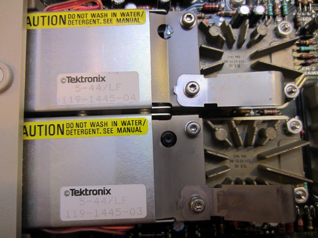
The CRT high voltage supply board (A9) is mounted inside a metal shielding can on the side of the CRT (see picture below). It is responsible for providing the -2 kV CRT control grid potential. The high voltage generator circuitry is contained inside the potted Murata module. This module is also responsible for generating the 14 kV CRT anode voltage.
Generally speaking, you should avoid touching any components in a high voltage circuit as lethal high voltages may still be present even long after power has been removed. It is not only just for your own safety, but for the safety of the components as well. Discharging through body resistance from a high voltage source to a sensitive component could permanently damage it.
|
|
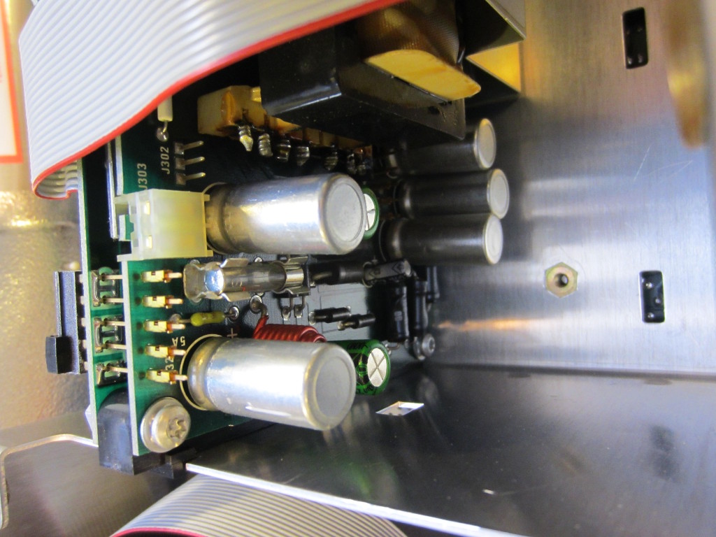
The picture to the right above is the picture of the low voltage regulator board taken from another angle, you can see all those linear regulators sitting on the heatsink at the bottom.
Here is a picture of the switching power supply board. All components interacting with mains voltage are tucked under the grounded aluminum shielding for added safety. The aluminum cover serves multiple purposes as well, as it is also a heatsink for the power components and a shield to prevent switching noises from entering the reset of the system.
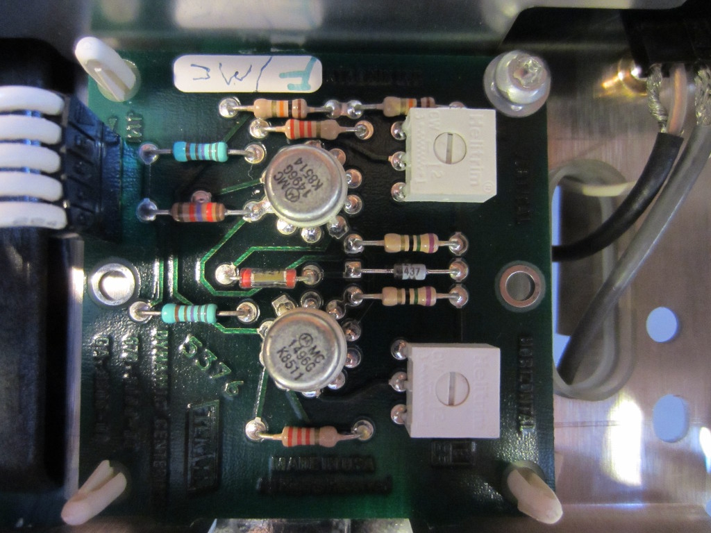
Here is a closeup of the dynamic centering board (A14). This board is mounted on the side of the CRT next to the shielded high-voltage power supply board.
From the datecodes present on the components, it appeared that this oscilloscope was manufactured sometime in 1985 and it had probably gone through a few revisions after 2465’s initial release in 1984.
Mounted vertically towards the other side of the oscilloscope is the A5 digital control board. This board controls most aspects of the scope via the on-board firmware.
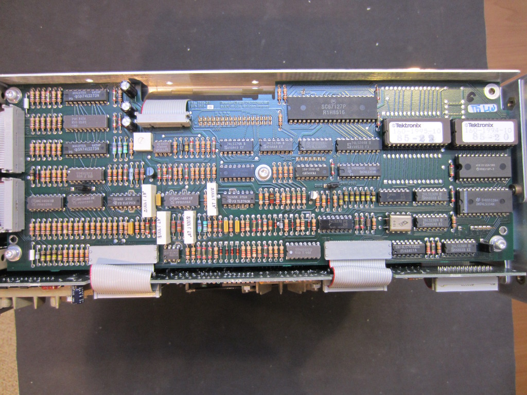
The main processor used here is a Motorola SC-67237P. If you looked at the PCB layout you will see that there are four designated footprints for 4 8K EPROMs for firmware storage. As you can see in the picture below, it is likely that this unit used two 16K EPROMs instead of four 8K EPROMs and hence the two empty footprints for the additional EPROM chips.
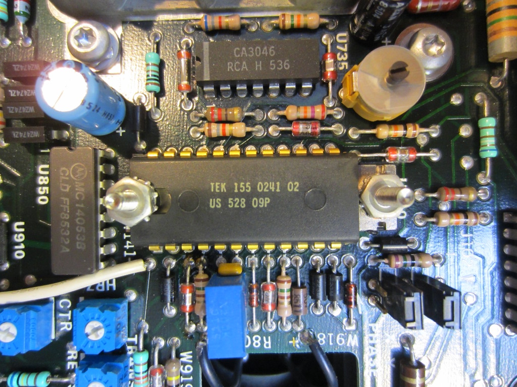
Here are two more close-up pictures of the A5 control board. As you can see, many of the ICs used on this board are ceramic packaged for enhanced heat conductivity and reliability. The second ceramic chip from the top marked 156-1589-00 is AM6012, a 12-bit high speed DAC.
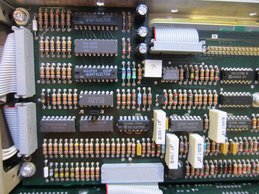
The chip towards the middle left marked 156-1566-00 shown in the picture below is an EAROM (electrically-alterable read-only memory), which is used to store calibration constants and front-panel settings. This EAROM was built on MNOS (metal-nitride-oxide) technology which requires different logic levels than the standard TTL logic. A level-shifter utilizing the MC1413 Darlington array is used to interface this EAROM to the reset of the TTL logic.
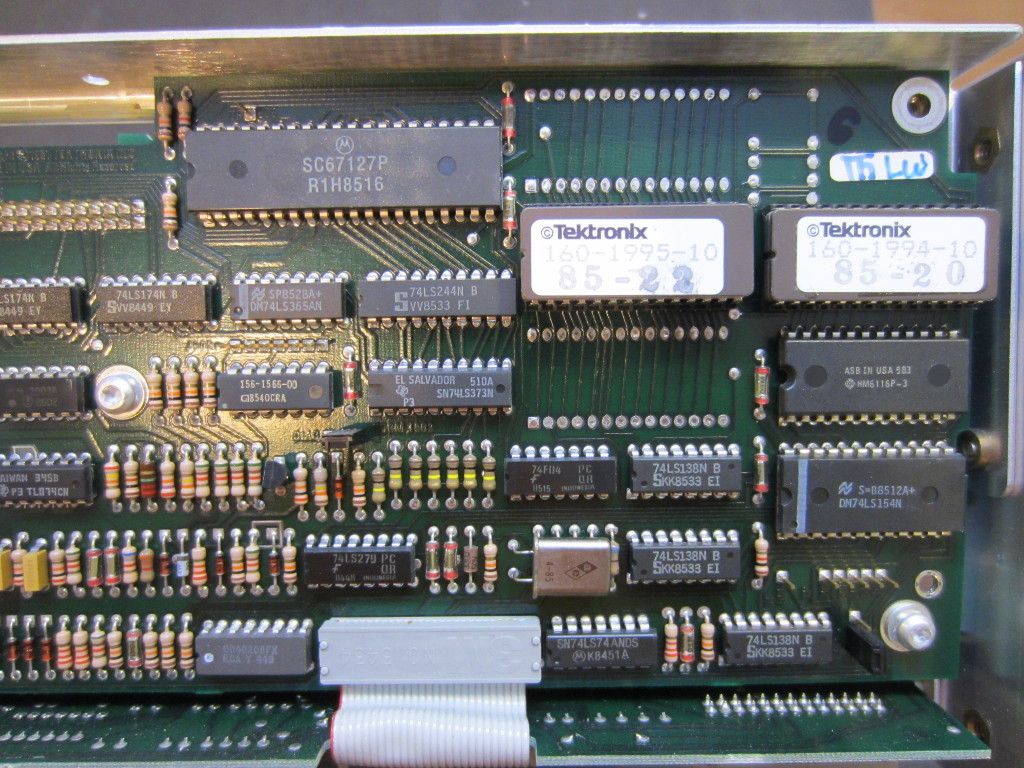
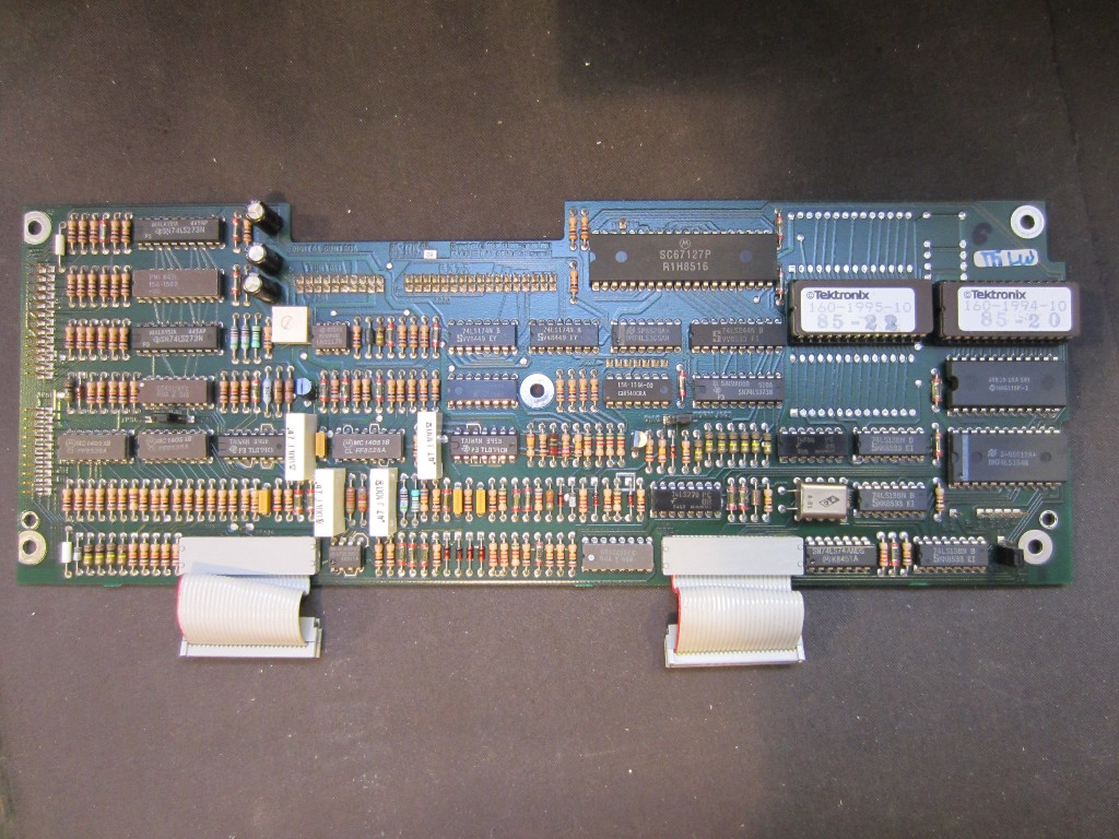
Here is another picture of the A5 board after it has been taken out of the chassis. This board connects to the front panel via the two headers located on the left side and connects to the main board (A1) on the bottom of the chassis via the two short ribbon cables. Like most Tektronix products, everything was designed with ease of serviceability in mind.
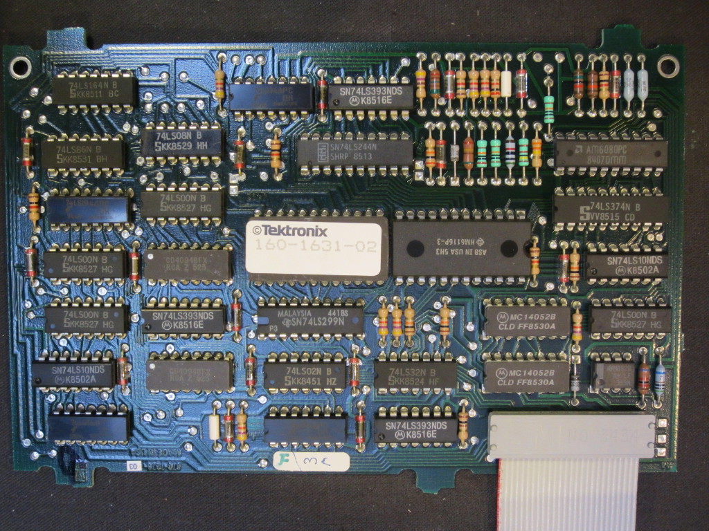
Here is a picture of the A6 digital readout board. This board is responsible for the on-screen information displays. The labeled chip in the center is the character ROM chip responsible for the generation of rasterized on-screen characters.
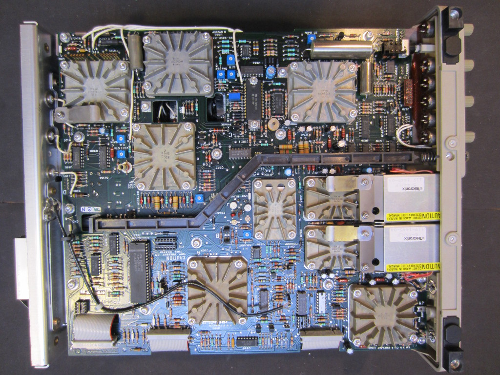
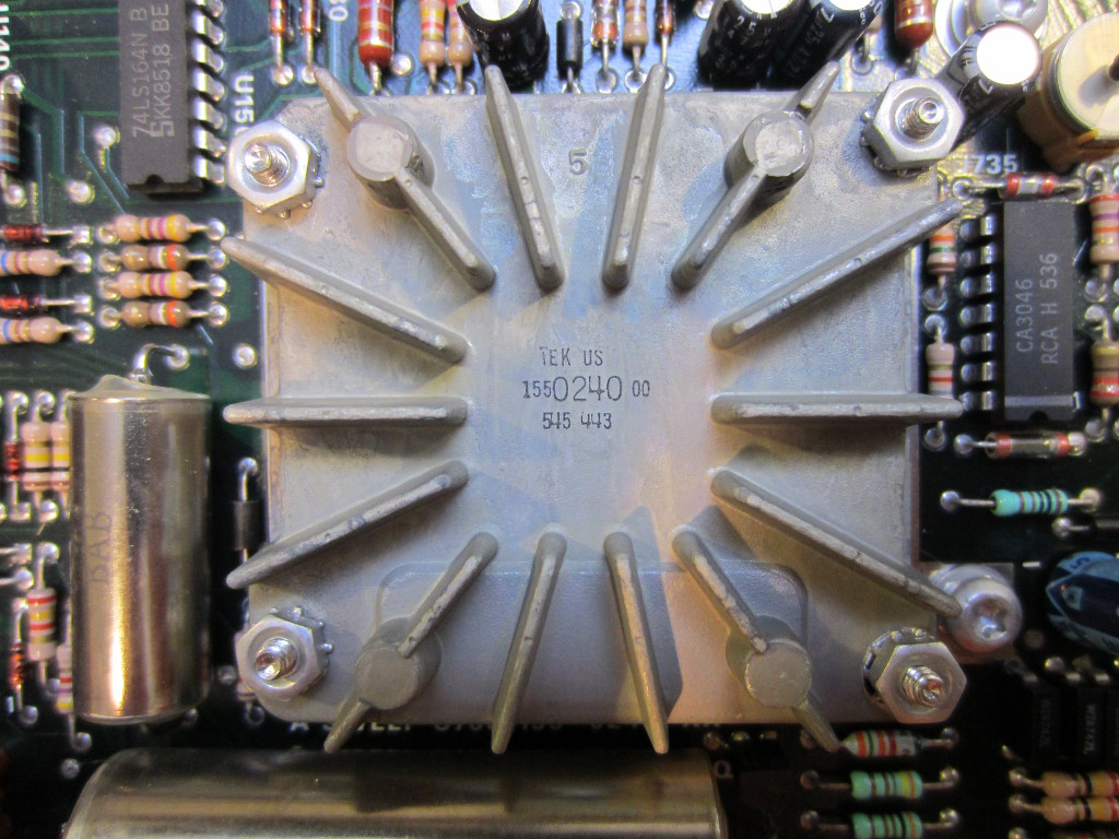
The mainboard (A1) is located at the bottom of the chassis, covering the entire bottom area. In the picture below, you can see quite a few heat-sinked custom hybrid modules specifically designed for the the 24×5 series scopes.
Care must be taken when servicing this board as many of the hybrid modules are very sensitive to ESD and also can overheat easily when there is no sufficient airflow. Should one of these hybrids fail, your best hope is to swap one from a donor scope since they have been discontinued long time ago.
|
|
Below is a picture of the “notorious” U800 horizontal amplifier IC. Many people had reported that this chip ran really hot and could potentially be destroyed if overheated.
Please note that the thermal design by Tektronix engineers requires adequate airflow to cool these components at all times. So overheating would only be an issue if the unit is in service mode with the cover removed. As without the cover, the air flow generated by the rear fan would no longer be present and in this case an external fan must be used to maintain the proper airflow and to ensure all components are operating under the safe thermal envelope.
So If you are really concerned, you could add a glue-on heatsink to U800. But it is not necessary as long as the service procedures are properly followed.
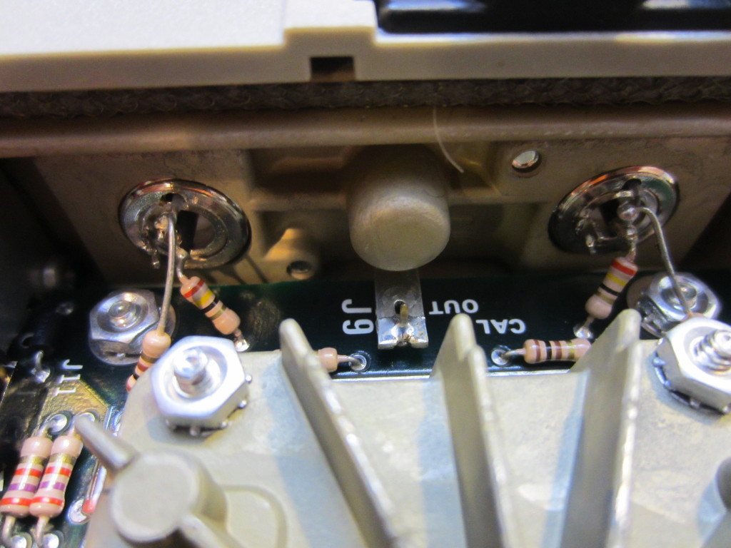
The picture blow shows the channel one and channel two input attenuators. These processor controlled attenuators are only available for these two channels. Attenuation on channel three and channel four are fixed at either 0.1V/div or 0.5v/div.
[adsense]
This picture shows the input circuitry of channel three and channel four.
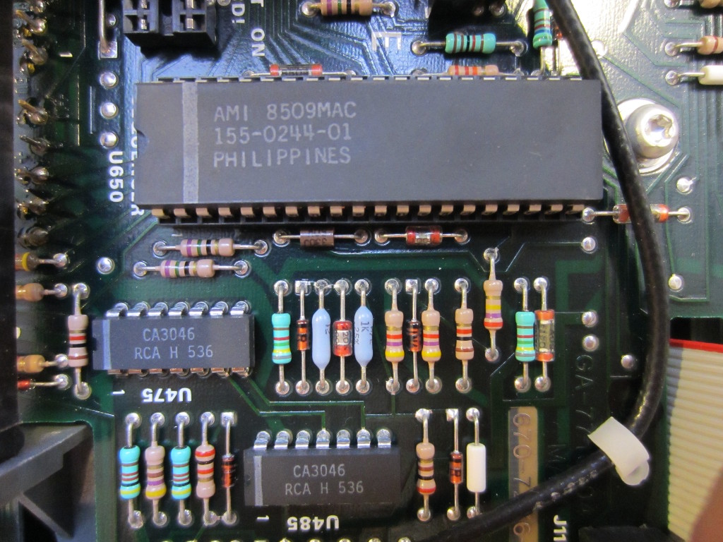
In the picture below you can see a rare ceramic packaged LM358.
The potentiometers located on the front panel are connected to the main board via flat-flex cable. In some earlier manufactured boards (like the ones used in my 2445), the connections were made using standard wires.
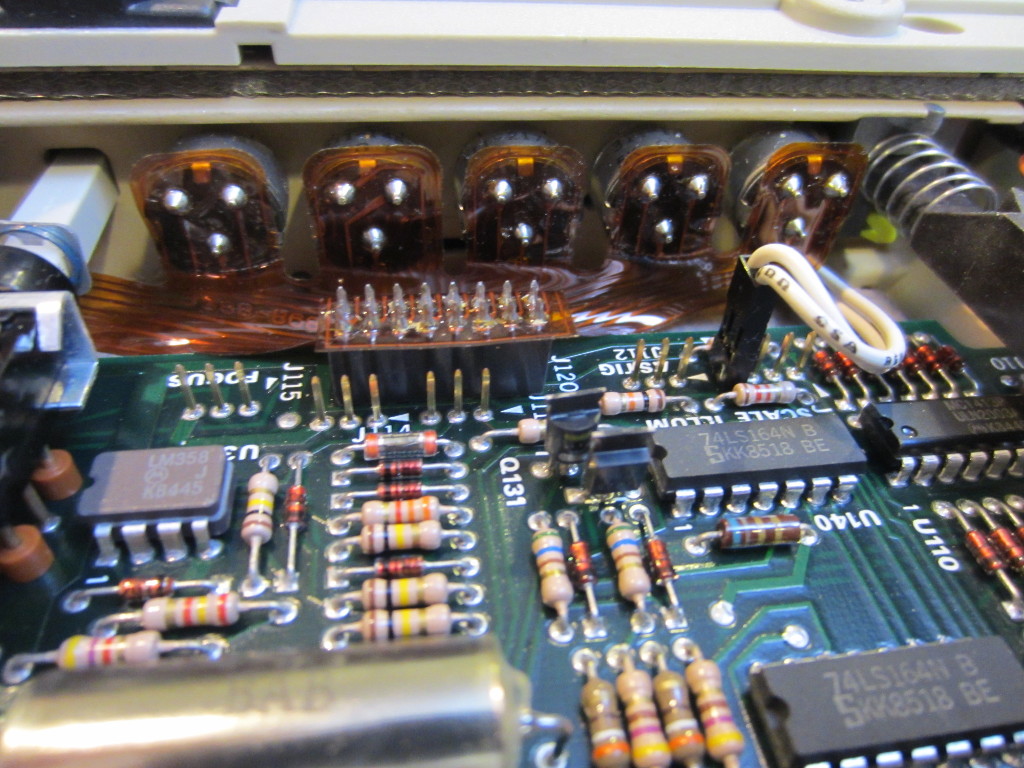
The picture below shows the display sequencing IC, which is responsible for all the on-screen information displays.
Because the mains power enters the unit from the rear panel, the power switch is controlled by a lever running the entire length of the circuit board from the front panel. This lever in turn pushes the switch located on the other side of the board. This layout prevents having to run cables carrying mains voltage all the way across the system and was quite common in other test equipment made in the same era. In the picture below, you can also see a ferrite bead over a signal cable, the ferrite bead is used to remove high frequency noises from the signal.
This picture below shows the measurement of a sinusoidal signal at the rated bandwidth limit of 300 MHz. For this measurement, the signal was DC coupled using 50 Ohm termination.
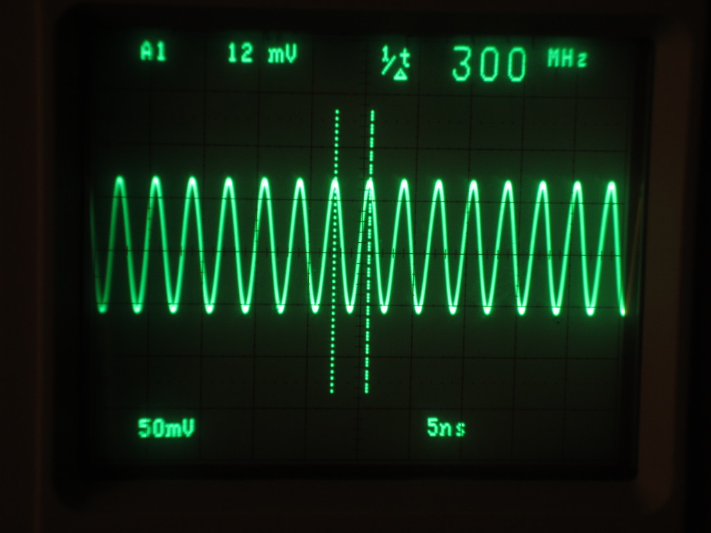
Of course, the result is exactly what we would expect for a nice and clean display.
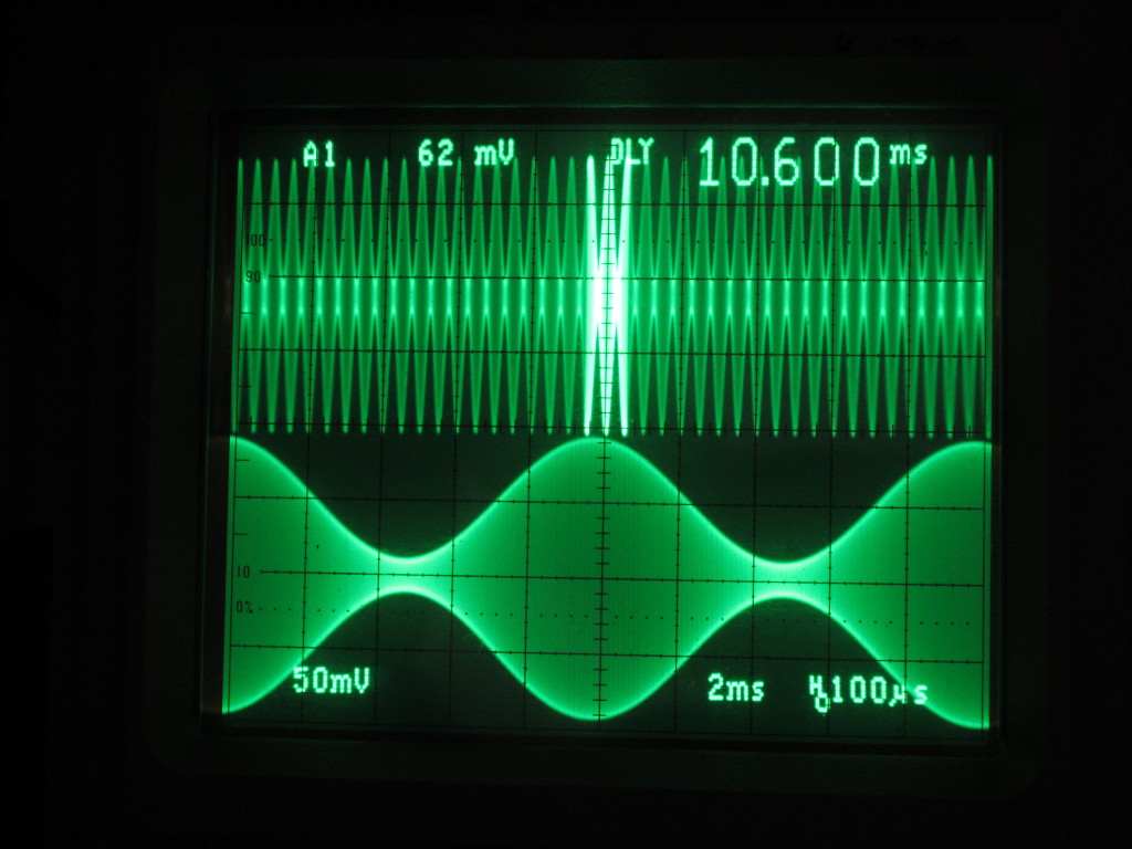
Here is a picture demonstrating the usage of delayed sweep. In this setup, an 85% amplitude modulated 1 kHz audio signal with a carrier frequency of 100 MHz is present at channel one. Many scopes (including some lower end modern DSOs) would have trouble triggering on modulated signals like this, but Tektronix 2456 can handle it with ease. The detailed AM modulation waveform corresponds to the highlighted portion in the coarse waveform above.
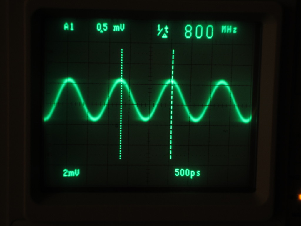
While for the 2465 the specified bandwidth is 300 MHz for each channel, the electronics used in the front-end is capable of handling much higher frequencies. Of course the amplitudes will be severely attenuated when measuring signals beyond the rated bandwidth and the shapes of the waveforms will no longer be accurate due to the limitation in rise time.
But being able to view signals beyond the designed frequency range is sometimes useful when you just need to get a reading of the circuit under measurement to see whether it is oscillating properly and if so what the oscillation frequency is.
Pushing the limit way beyond the rated operating frequency of the front-end amplifier is only possible on an analog scope. As for a digital scope, while the front-end might be able to amplify the signal, the limit in sampling rate would cause signal aliasing. And if the displayed waveform is aliased, you will no longer be able to get the true frequency of the signal under test.
Below is a picture showing the measurement of an 800 MHz waveform using the x10 magnification function with a 5ns/div horizontal sweep rate (effectively 500ps/div). Note that while the signal is significantly attenuated and becomes a little bit blurry, the frequency measurement nevertheless remains quite accurate. For this particular scope, it is possible to measure frequencies all the way up to just below 1 GHz.
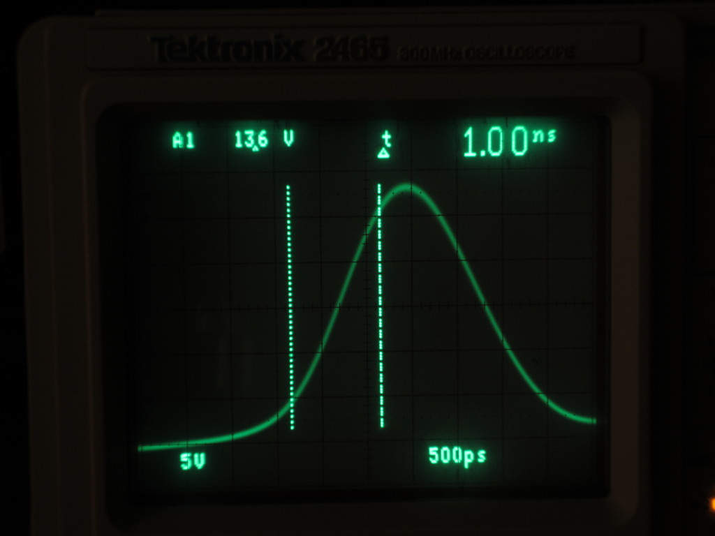
Using an extremely fast rising pulse generated via an avalanche pulser, we can test the rise time of the scope and thus verify its bandwidth claim. Here the rise time of the pulse measured is at 1 ns (from 10% to 90% in amplitude), which corresponds to a bandwidth of 350 MHz (BW=0.35/Tr) just above the specified 300 MHz bandwidth.