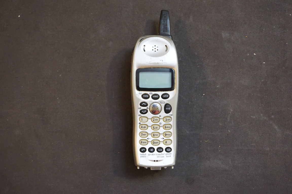
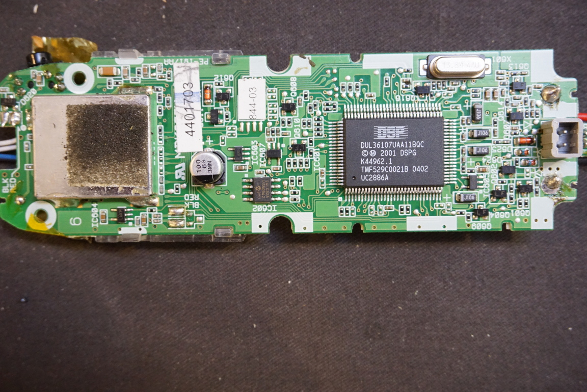
I recently upgraded my home phone system and thus was left with a couple of old Uniden DCT648-2 handsets. Most of the components inside are probably not salvageable but these handsets use 3×16 character LCDs, so it would be nice if I could reuse them in my other projects.
|
|
The LCD inside the DCT648-2 handset has 8 pins. This suggests that it is using some kind of serial protocol. Unfortunately, I could not find any information on the LCD used here so I decided to hook it up to a logic analyzer and see if I could reverse engineering the protocol used to drive the LCD.
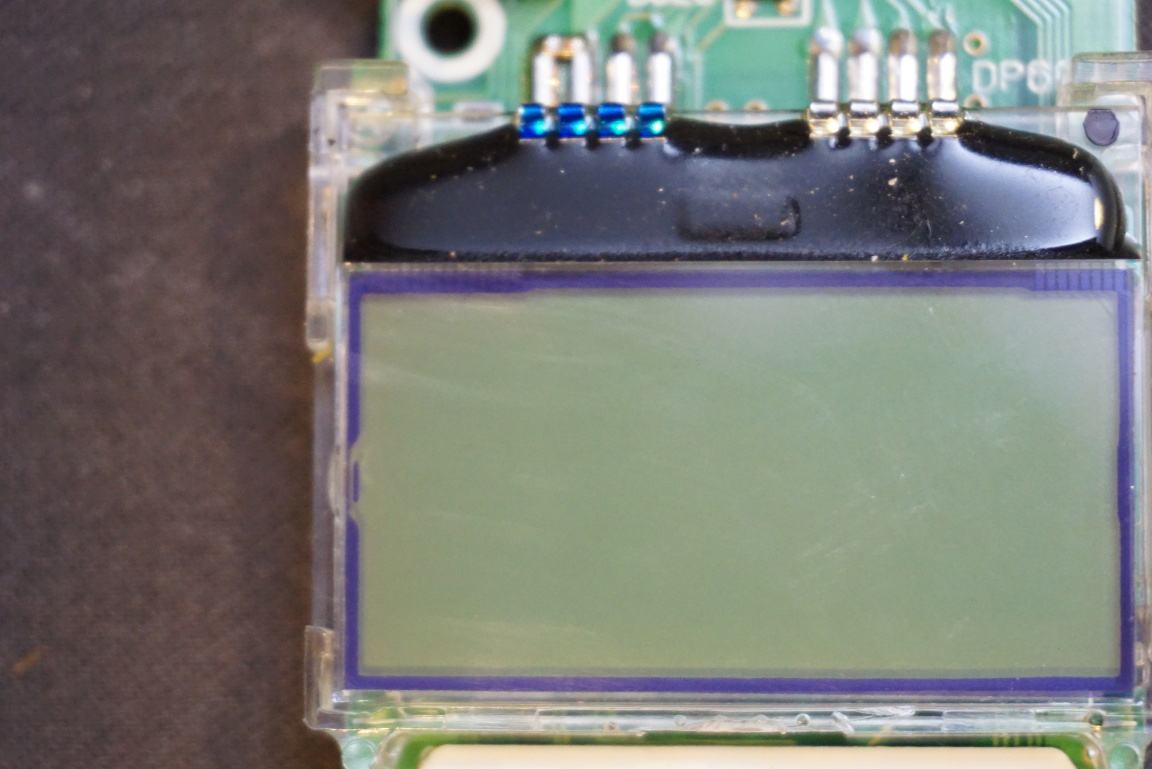
A few of the pins can be easily identified. Pin 2 (from left to right) is clearly connected to the circuit ground. And pin 3 measures 3.3V when the phone is powered on which suggests that the LCD uses 3.3V logic. Pin 1 is roughly -2.6 with respect to the ground. If you look at the PCB carefully, you will see a capacitor is placed between pin 1 and ground. Since there is no visible trace coming out from pin 1, I think it is used solely for connecting an external capacitor for the builtin charge pump to provide the negative voltage needed by the LCD.
With this information, I hooked up pin 2 through pin 8 to my logic analyzer. After looking at the captured data, it became clear that this LCD is using some kind of slightly modified SPI protocol. We can also easily identify that pin 6 is the SPI clock, pin 7 is the MOSI and pin 8 is the CS pin. From the captured data we can also see that the clock remains high when inactive (CPOL=1).
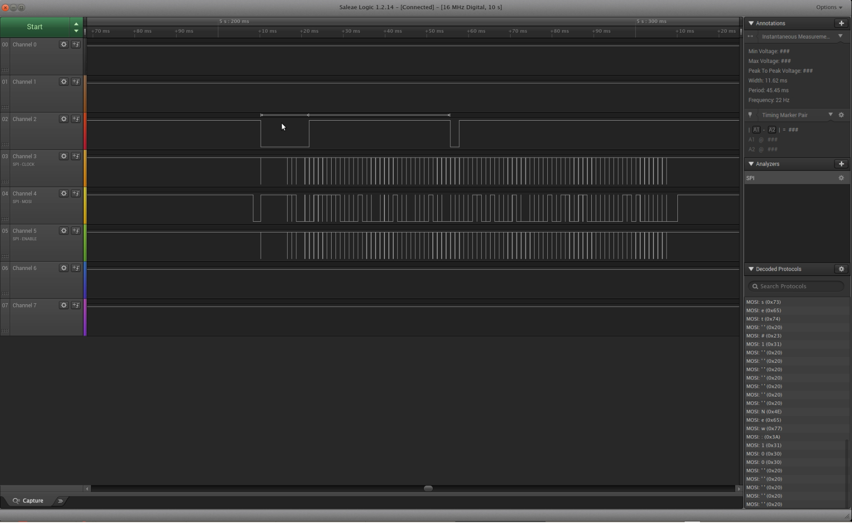
Pin 5 doesn’t look to conform to any standard SPI signal, but as you will see shortly it is presumably used to load command to initialize the LCD. Now the only question remaining is whether the data is loaded on the leading edge or the trailing edge of the clock.
After comparing the data captured using data valid on rising edge settings (CPHA=0) and data valid on trailing edge settings (CPHA=1) it became clear that CPHA=1 is used as when setting CPHA to 0 the decoded output sometimes become garbled, which suggests that the signal is not yet settled on the rising edge.
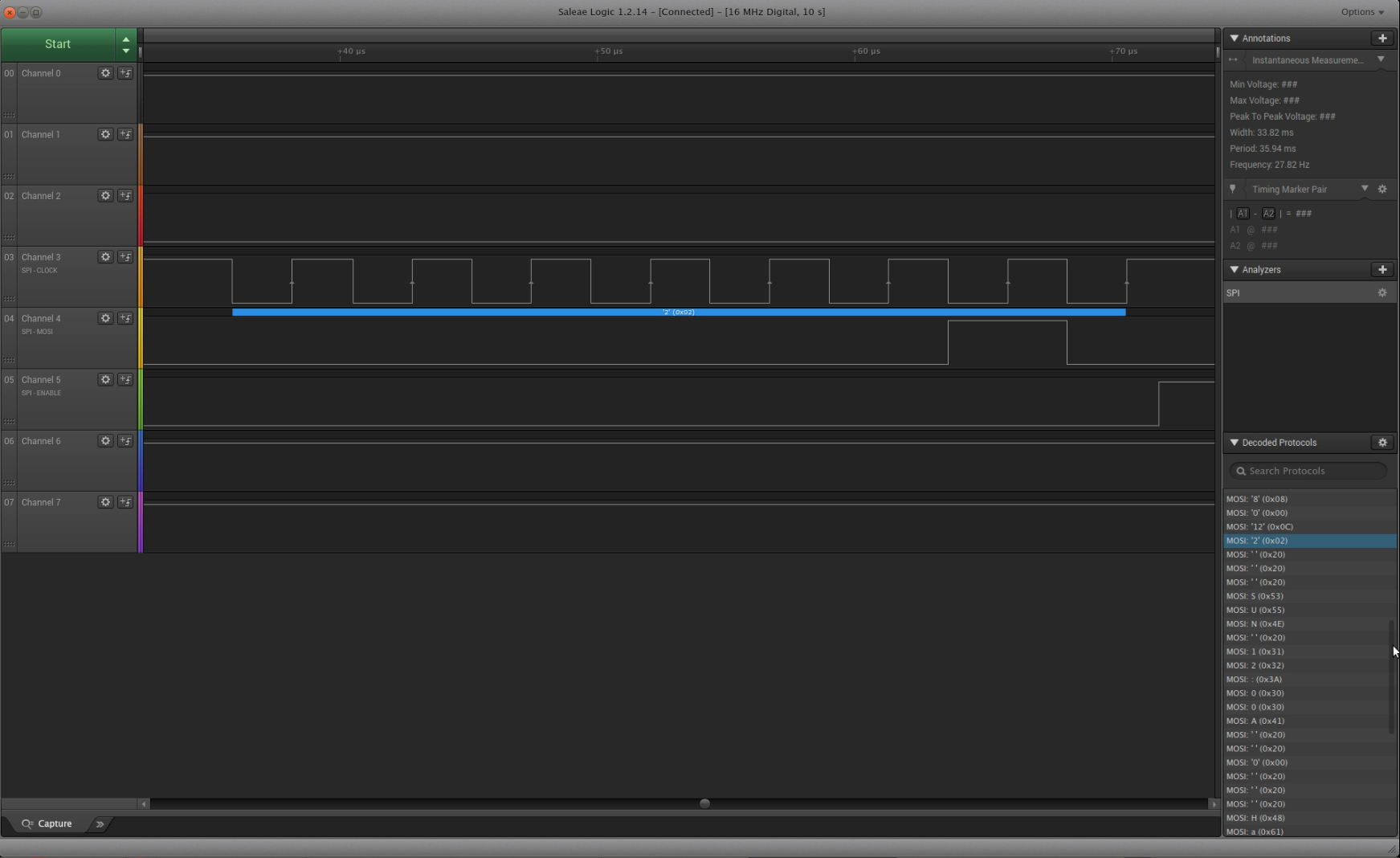
So now we know the SPI mode the LCD is communicating with: CPOL=1 and CPHA=1. This corresponds to SPI_MODE3 in Arduino. Since the character LCD is 3×16 (48 bytes) but each frame contains 87 bytes and the actual character displayed on the LCD starts from the 40th byte so the first 39 bytes must be some kind of initialization data that prepares the LCD for data display. The first 39 bytes also do not seem to change when the display changes. The 39th byte corresponds to the last low-to-high transition of pin 2 so clearly pin 2 is used to signify the beginning of the display data.
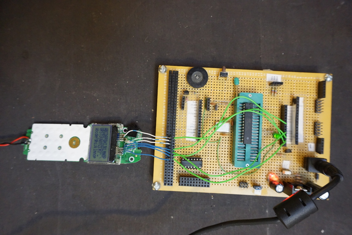
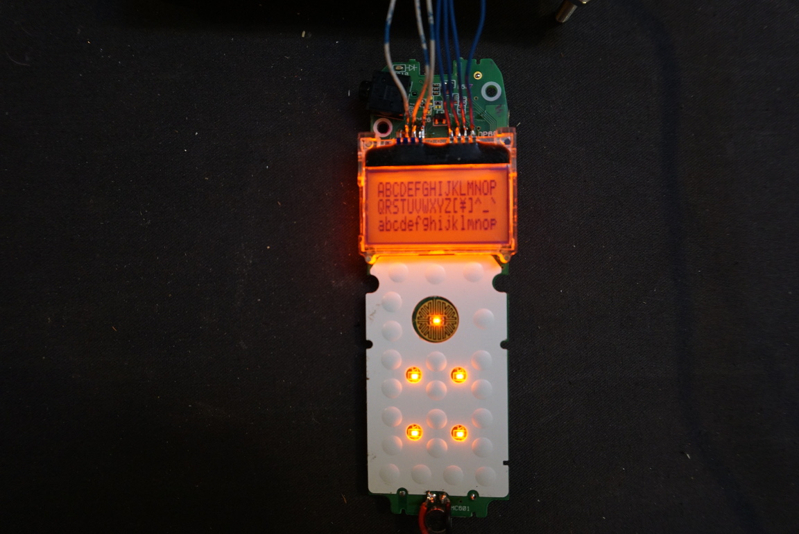
To test whether the above assumptions are correct, I used a 3.3V powered Arduino prototyping board I built a while back and wrote a simple program (see below). The code basically just output ASCII characters from 65 (“A”) and upwards until it fills all 48 spaces on the screen.
Instead of mounting the LCD onto a protoboard, I simply cut the signal traces and used an ATMega328p running Arduino to talk to the display.
And here is a screenshot of the output.
The corresponding code I used is listed below, the 39 bytes header info is somewhat mysterious but it seems to be working just fine by sending these verbatim each time with the correct timing and command pin toggle.
#include <SPI.h>

const int pinMOSI = 11; //MOSI
const int pinMISO = 12; //MISO
const int pinSPIClock = 13; //SCK
const int pinCS = 10; //CS
const int pinCmd = 9; //CMD

char header[] = {
0x31, 0x31, 0x31, 0x06, 0xc0, 0x0e, 0x11, 0x13, 0x17, 0x1f, 0x1f, 0x1f, 0x00,
0x04, 0x0e, 0x0e, 0x0e, 0x0e, 0x1f, 0x04, 0x00, 0x00, 0x02, 0x15, 0x05, 0x15,
0x02, 0x00, 0x00, 0x00, 0x1b, 0x12, 0x1b, 0x12, 0x12, 0x00, 0x00, 0x0c, 0x02};

void setup() {
  Serial.begin(9600);
    pinMode(pinMOSI, OUTPUT);
    pinMode(pinMISO, INPUT);
    pinMode(pinSPIClock, OUTPUT);
    pinMode(pinCS, OUTPUT);
    pinMode(pinCmd, OUTPUT);

    digitalWrite(pinCS, HIGH);
    digitalWrite(pinCmd, HIGH);

    SPI.begin();
    SPI.setDataMode(SPI_MODE3);
}

void writeCmd()
{
  digitalWrite(pinCmd, LOW);

  digitalWrite(pinCS, LOW);
  SPI.transfer(header[0]);
  digitalWrite(pinCS, HIGH);
  delayMicroseconds(180);

  digitalWrite(pinCS, LOW);
  SPI.transfer(header[1]);
  delayMicroseconds(30);
  digitalWrite(pinCS, HIGH);

  digitalWrite(pinCS, LOW);
  SPI.transfer(header[2]);
  digitalWrite(pinCS, HIGH);
  delayMicroseconds(30);

  digitalWrite(pinCS, LOW);
  SPI.transfer(header[3]);
  digitalWrite(pinCS, HIGH);
  delayMicroseconds(60);

  digitalWrite(pinCS, LOW);
  SPI.transfer(header[4]);
  digitalWrite(pinCS, HIGH);
  delayMicroseconds(30);

  digitalWrite(pinCmd, HIGH);

  for (int i = 5; i < 37; i++) {
    digitalWrite(pinCS, LOW);
    SPI.transfer(header[i]);
    digitalWrite(pinCS, HIGH);
    delayMicroseconds(30);
  }

  digitalWrite(pinCmd, LOW);

  digitalWrite(pinCS, LOW);
  SPI.transfer(header[37]);
  digitalWrite(pinCS, HIGH);
  delayMicroseconds(30);

  digitalWrite(pinCS, LOW);
  SPI.transfer(header[38]);
  digitalWrite(pinCS, HIGH);
  digitalWrite(pinCmd, HIGH);
  delayMicroseconds(30);
}

void writeData()
{
  for (int i=0; i<48; i++) {
    digitalWrite(pinCS, LOW);
    SPI.transfer(i+65);
    digitalWrite(pinCS, HIGH);
    delayMicroseconds(30);
  }
}

void loop() {
  writeCmd();
  writeData();
  delay(20);
}
Finally, here is a video showing the process of this reverse engineering, you can find more information of analyzing the protocol used by this LCD in the video.

