Arbitrary waveform generators come in handy when troubleshooting digital and analog circuits. Most commercial arbitrary waveform generators are very expensive due to the functionality and very high bandwidth they offer. But for typical uses among hobbyists, the requirements are generally pretty low. Building a very basic arbitrary waveform generator is actually quite simple using a digital-to-analog converter (DAC) chip and a microcontroller (MCU). Here I will show you one such waveform generator using Linear Technology‘s LTC1450 DAC and ATmega328 programmed with Arduino libraries.
For general usage, you can pretty much use any DAC chip. But for better performance, a parallel interface DAC should be used since the digital input bits can be loaded simultaneously rather than being shifted in one by one. The conversion time of the DAC dictates the maximum achievable frequency.
Most of the mainstream DAC chips nowadays can operate at more than 100 kHz. Keep in mind though that the number of bits used as waypoints to generate the output waveform also affects the maximum achievable frequency. So a 12 bit DAC that can operate at 100 kHz and output a square wave up to 100 kHz (1bit) may only be able to generate a 25 Hz signal if all the 12 bits are used as waypoints. In general though, we rarely use more than a few hundred waypoints so the typical operating frequencies that can be achieved are well above 1 kHz which is more than adequate in most cases.
In this example, a 12 bit DAC (LTC1450) is used. It can operate stably at 200 kHz (1 bit) and the full resolution (12 bit) waveform frequency is around 50 Hz.
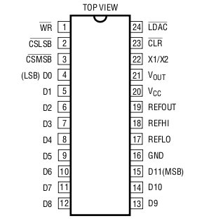
The wiring for this DAC is very straightforward. As you can see in the sample code below, the parallel input interface (D0-D11) is connected with 12 of ATmega328’s digital and analog pins (the analog pins are used as digital outputs as well). In addition to DAC’s input pins, three additional pins are used to control the DAC.
#include <TimerOne.h>

const int pinD0 = 14; //PC0; -- D0
const int pinD1 = 15; //PC1; -- D1
const int pinD2 = 16; //PC2; -- D2
const int pinD3 = 17; //PC3; -- D3
const int pinD4 = 18; //PC4; -- D4
const int pinD5 = 19; //PC5; -- D5

const int pinD6 = 2; //PD2;  -- D6
const int pinD7 = 3; //PD3;  -- D7
const int pinD8 = 4; //PD4;  -- D8
const int pinD9 = 5; //PD5;  -- D9
const int pinD10 = 6; //PD6; -- D10
const int pinD11 = 7; //PD7; -- D11
const int pinCSLMSB = 12; //PB4; -- CSLSB, CSMSB
const int pinWR = 11; //PB3;
const int pinLDAC = 10; //PB2;

unsigned int counter = 0;

void setup()
{
  //LTC1450 ADC output pins
  pinMode(pinD0, OUTPUT);
  pinMode(pinD1, OUTPUT);
  pinMode(pinD2, OUTPUT);
  pinMode(pinD3, OUTPUT);
  pinMode(pinD4, OUTPUT);
  pinMode(pinD5, OUTPUT);
  pinMode(pinD6, OUTPUT);
  pinMode(pinD7, OUTPUT);
  pinMode(pinD8, OUTPUT);
  pinMode(pinD9, OUTPUT);
  pinMode(pinD10, OUTPUT);
  pinMode(pinD11, OUTPUT);

  //LTC1450 control pins
  pinMode(pinCSLMSB, OUTPUT);
  pinMode(pinWR, OUTPUT);
  pinMode(pinLDAC, OUTPUT);

  digitalWrite(pinCSLMSB, HIGH);
  digitalWrite(pinWR, HIGH);
  digitalWrite(pinLDAC, HIGH);

  digitalWrite(pinCSLMSB, LOW);
  digitalWrite(pinWR, LOW);

  //set timer interval to 100ns
  //the output frequency is determined byinputs
  //the number of sample points used in the DAC
  //in this example, 8 values are used and thus
  //the frequency is roughly 1s/800ns.
  //The actual frequency is slighly lower
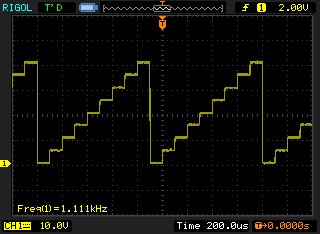
  //(in this case 1.1 khz)
  Timer1.initialize(100);
  Timer1.attachInterrupt(onTimer);
}

void onTimer()
{
  //CSLSB/CSMSB=0, WR=0;
  PORTB &= ~(_BV(PB4) | _BV(PB3));

  //set the lower 6 bits (bit 0 to 5)
  //which corresponds to PC0 to PC5
  PORTC = (counter & 0x3F);

  //set the higher 6 bits (bit 6 to bit 11)
  //the value is right shifted by 4 since the first
  //port in PORTD we use is PD2
  PORTD = (counter & 0xFC0)>>4;

  //CSLSB/CSMSB=1, WR=1;
  PORTB |=  _BV(PB4) | _BV(PB3);

  //Load DAC
  PORTB &= ~_BV(PB2);
  PORTB |= _BV(PB2);

  //generate 8 staircases
  counter += 500;

  //reset counter
  if (counter >= 4096) counter = 0;
}

void loop()
{
}

Note that both CSLSB and CSMSB of LTC1450 are connected together to enable parallel loading of all 12 bits.
For maximum efficiency, I used AVR routines within the timer routine directly as they are significantly faster than the corresponding Arduino functions. For the setup() routine, I used Arduino functions since speed is not an issue as they are called only once and the pin assignment can be seen a bit more clear.
I used the 16 bit timer interrupt for precise DAC timing. If the timing requirement is not critical, bitbanging method can also be used. The pins are arranged in such a way that 6 bits are mapped to PORT C pins and 6 bits are mapped to PORT D pins and the bit ordering is the same order (i.e. low to high) as in the corresponding ports. This arrangement is necessary to ensure all 12 bits can be loaded with just two instructions:
  PORTC = (counter & 0x3F);
  PORTD = (counter & 0xFC0)>>4;
Other pin arrangements are also possible but will require more instructions to load and thus reduce the maximum achievable waveform frequency. The output frequency can be controlled in two places. The first place is the timer interval and the second place is the number of bits used to represent each waveform. While the example above only shows the generation of a fixed staircase signal, other arbitrary waveforms of varies frequencies can be easily achieved by modifying the onTimer portion of the code.
Here is the oscilloscope output from the signal generated above.


