In my earlier posts (1, 2, 3), I showed some examples of using the I2C protocol with TI’s MSP430 Launchpad. Many MCUs in the MSP430G2 family also support the SPI bus. In today’s discussion, I will give a couple of examples on communicating with an SPI port expander (MCP23S17).
Dave has written a great tutorial on the theory behind the SPI protocol. He also has provided many in-depth examples on how to use SPI with TI’s MSP430G2 Launchpad. So I won’t elaborate much on the protocol itself here.
SPI is arguably a much simpler protocol compared to I2C. From an SPI master device’s stand point, all it needs to do is to select the device it wants to talk to (e.g. via CS pin) and clock the data out via the MOSI pin. If there is return value from the slave device, by simply applying additional clocks the returned value will be clocked out from the MISO pin.
But almost all of the examples I found (including TI’s own sample code) use interrupt exclusively for handling the SPI calls. Unfortuantely, the use of interrupt routines made the examples more complicated than necessary. Nevertheless, using interrupts is actually the preferred approach as the program does not need to be spin-waiting for the data transfer and could save valuable CPU cycles. Also, this approach enables the MCU to enter low power mode in between requests which keeps the power consumption down to a miminal. The low-power feature is essential to battery powered devices.
For straight-forward illustration of how to use SPI on MSP430G2, I thought I would give a couple of “cleaner” SPI examples that do not rely on interrupts. People who are familiar with Arduino programming should find my examples easier to follow. The MCU I used in here is MSP430G2231, but any chip in the MSP430G2 line that supports SPI can also be used. The chip we are communicating with is a MCP23S17 16 bit SPI port expander from Microchip.
In the following code snippets, CS is tied to P1.4 and is setup via P1_init(). USI_init() setups the MCU in SPI mode (largely Dave’s code with some modifications to clock speed). The full code listing can be downloaded towards the end of the post.
SPI – Sending data
The command format we are using is as follows, altogether 32 bits of command data is sent to MCP23S17.
Device Opcode, Rgister Address, GPIO Value (16 bit)
The SPI call is initialized by pulling down CS. And each chunk of data (either 8 bits or 16 bits) is sent with the folloing statements:
	USISRL = 0x40; //device opcode 0100 (Fixed for MCP23S17) 000 (MCP23S17 Address) 0 (write)
	USICNT = 8; //number of bits
	while (!(USIIFG & USICTL1)); //wait till the transfer is complete
The first SPI command (between P1OUT &= ~CS and P1OUT |= CS) sets MCP23S17’s port as output. Within the for loop, a 16-bit counter is incremented and then outputted to the 16 GPIO port. Finally after all 4 commend bytes are transmitted, the CS line is asserted to deselect the device indicating the end of the SPI call.
If you hook up some LEDs on the GPIO pins, you will see them light up following the binary representation of the counter.
void main(void) {
	unsigned int w = 0;

	WDTCTL = WDTPW + WDTHOLD;
	P1_init(); //initialize port
	USI_init(); //initialize USI to SPI

	P1OUT &= ~CS; //select chip

	//0100 000 0
        //0100 Fixed for MCP23S17
	//address pins A2 A1 A0 are 000
        //0 write
	USISRL = 0x40;
	USICNT = 8;
	while (!(USIIFG & USICTL1));

	//By default IOCON = 0
	//Write to IO direction register
	USISRL = REG_ADDR_IODIRA;
	USICNT = 8;
	while (!(USIIFG & USICTL1));

	//set all directions to OUTPUT (default is input)
	USISR = 0x00;
	USICNT = USI16B + 16;
	while (!(USIIFG & USICTL1));

	P1OUT |= CS; //de-select the chip

	for (;;) {
		P1OUT &= ~CS;

		//01000000
		//address pings A2 A1 A0 are 000
		USISRL = 0x40;
		USICNT = 8;
		while (!(USIIFG & USICTL1));

		//Write to Port B
		USISRL = REG_ADDR_GPIOB;
		USICNT = 8;
		while (!(USIIFG & USICTL1));

		//Writing 16 bits
		USISR = w;
		USICNT = USI16B + 16;
		while (!(USIIFG & USICTL1));

		P1OUT |= CS;
		w++;
		__delay_cycles(100000l);
	}
}
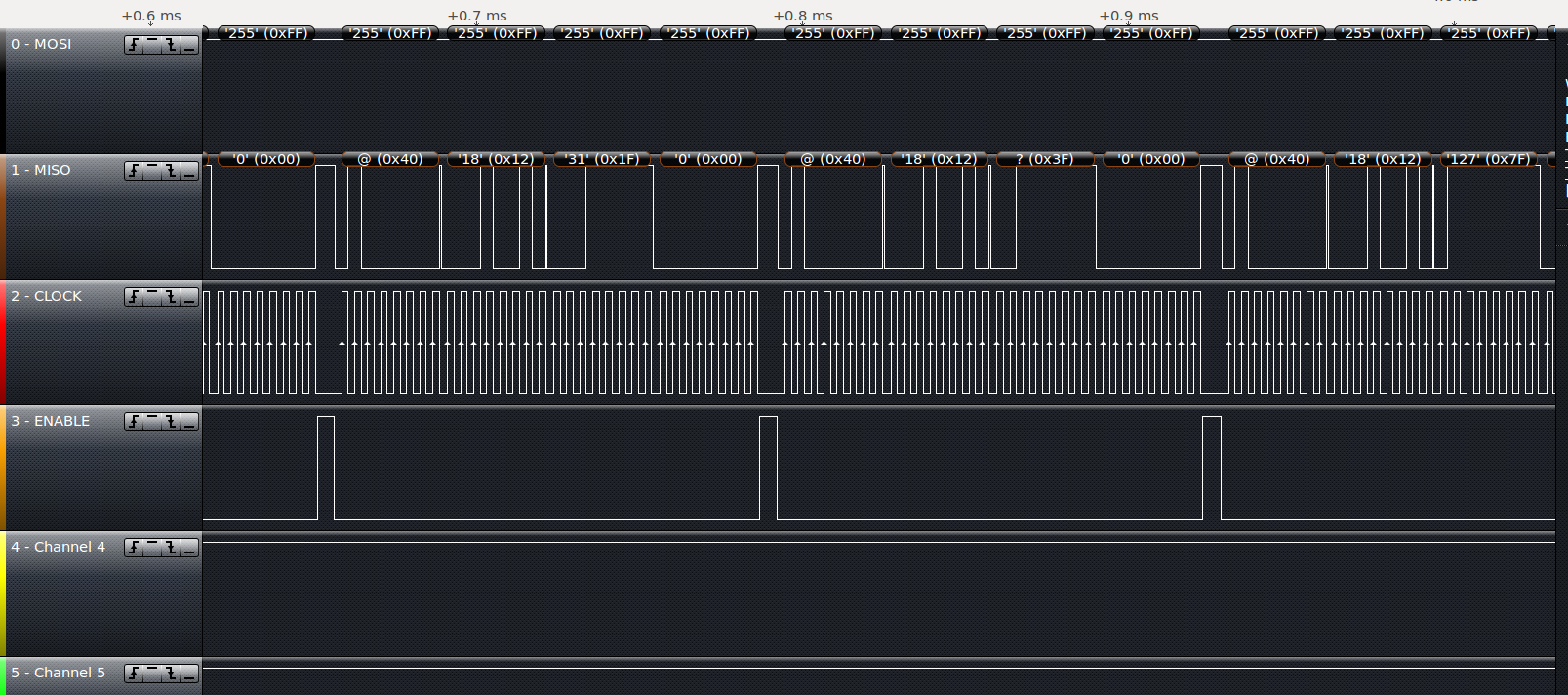
The following graph shows the logic analyzer capture of the waveforms on MISO, MOSI, CLOCK and EN pins.
SPI — Receiving data
Receiving the data from the SPI bus can be done in a similar fashion. In the first SPI command, the 16 GPIO ports of MCP23S17 are setup as input. Within the for loop, a read command is sent to MCP23S17. Following the read command, register REG_ADDR_GPIOA is sent. Even though we only indicated that we wanted to read from GPIOA, GPIOB will be read if more clocks are present after reading GPIOA’s 8 bits. Since USICNT is set to 16, both GPIOA and GPIOB’s contents are clocked out. Note that the content of USISRL is not important (set to 0 in the code below) when we send the SPI command as we only care of about the results coming back. After the SPI command finishes, USISR contains the 16bit results read from MCP23S17’s GPIO ports. The higher eight bits are for GPIOA and the lower eight bits are for GPIOB.
void main(void) {
	WDTCTL = WDTPW + WDTHOLD;
	P1_init();
	USI_init();

	P1OUT &= ~CS;

	//01000000
	//address pins A2 A1 A0 are 000
	USISRL = 0x40;
	USICNT = 8;
	while (!(USIIFG & USICTL1));

	//By default IOCON = 0
	//Write to IO direction register
	USISRL = REG_ADDR_IODIRA;
	USICNT = 8;
	while (!(USIIFG & USICTL1));

	//set all directions to INPUT (default is input)
	USISR = 0xFF;
	USICNT = USI16B + 16;
	while (!(USIIFG & USICTL1));

	P1OUT |= CS;

	for (;;) {
		P1OUT &= ~CS;

		//0100 000 1
		//address pings A2 A1 A0 are 000, read
		USISRL = 0x41;
		USICNT = 8;
		while (!(USIIFG & USICTL1));

		//Write to Port A
		USISRL = REG_ADDR_GPIOA;
		USICNT = 8;
		while (!(USIIFG & USICTL1));

		//clock out 16 bits
		USISRL = 0;
		USICNT = 16;
		while (!(USIIFG & USICTL1));

		P1OUT |= CS;

		//w contains the bits read from MCP23S17
		w = USISR;

		__delay_cycles(100000l);
	}
}
In both examples, SPI mode 0 is used.
MCP23S17_SPI_2231.zip (Tested under CCS 5.2.1)

