This old Cisco switch was on its way to the dumpster at my work place, so I thought I would rescue it. After all, while there are plenty of teardowns of consumer grade networking gear on the internet, teardowns of enterprise level network equipment have been hard to come by. So at the very least it would be a good opportunity to take a good peek inside.
The Cisco CSS 11503 content services switch was manufactured back in 2002, the year Pentium 4-M was first released. Considering the life span of your typical computing gear, this is really an ancient artifact from the dinosaur age.
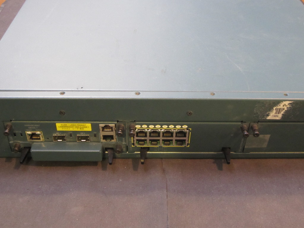
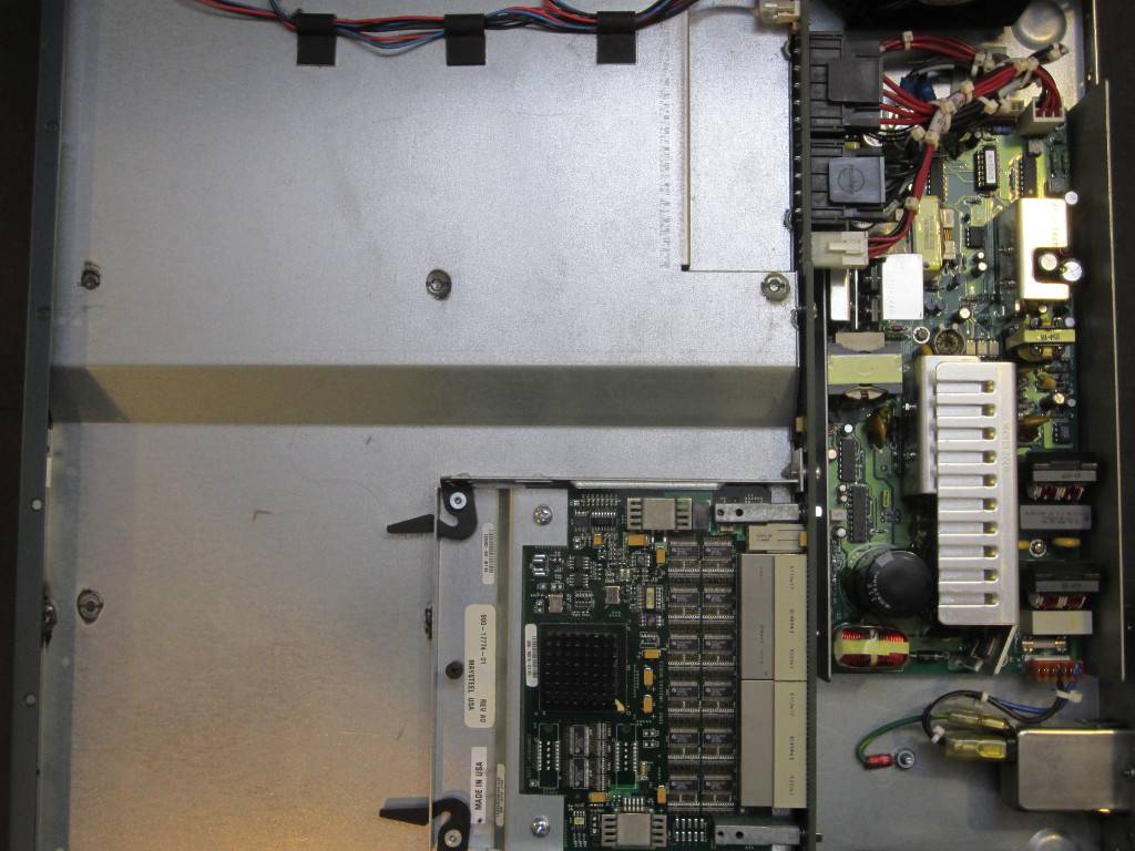
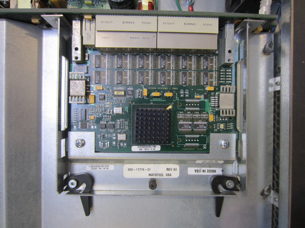
This unit is equipped with both a fast ethernet switch module and a dual port fiber optics module. The third expansion bay is unused. The picture below to the right shows the inside after the removal of the top cover. In this picture we can see the switching power supply board at the end and a control board on top sitting in the middle.
|
|
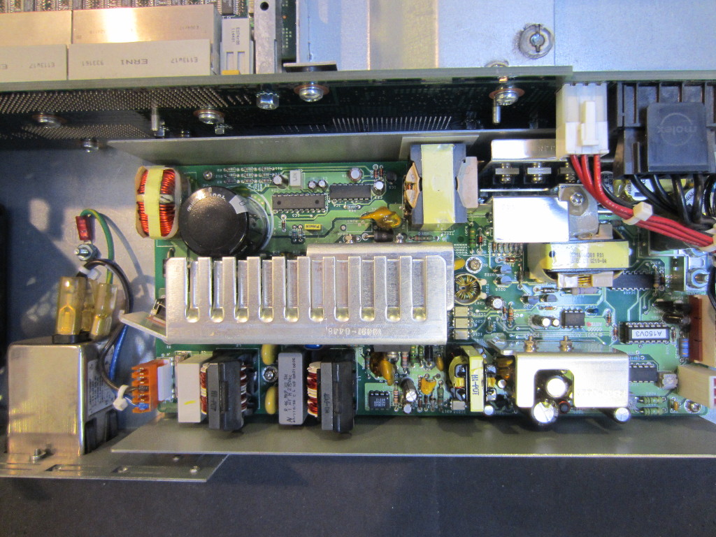
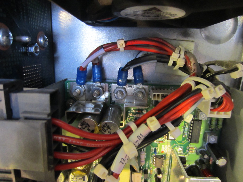
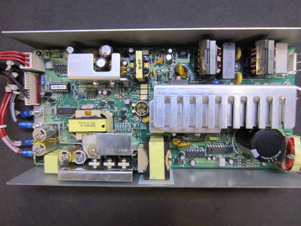
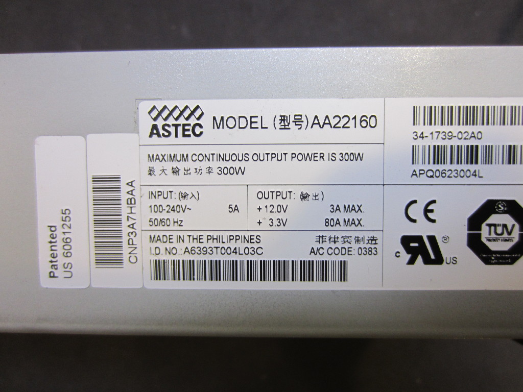
Like many test gear made back then, the entire case was made of sheet steel. So the case is very sturdy and can definitely survive a few feet drops. But on the other hand, these cases are extremely heavy. In the pictures below, you can see the switching supply PCB board and a closeup of the output terminals. The 3.3V rail supplies most of the power and the rated current for the 3.3V supply is 80A.
|
|
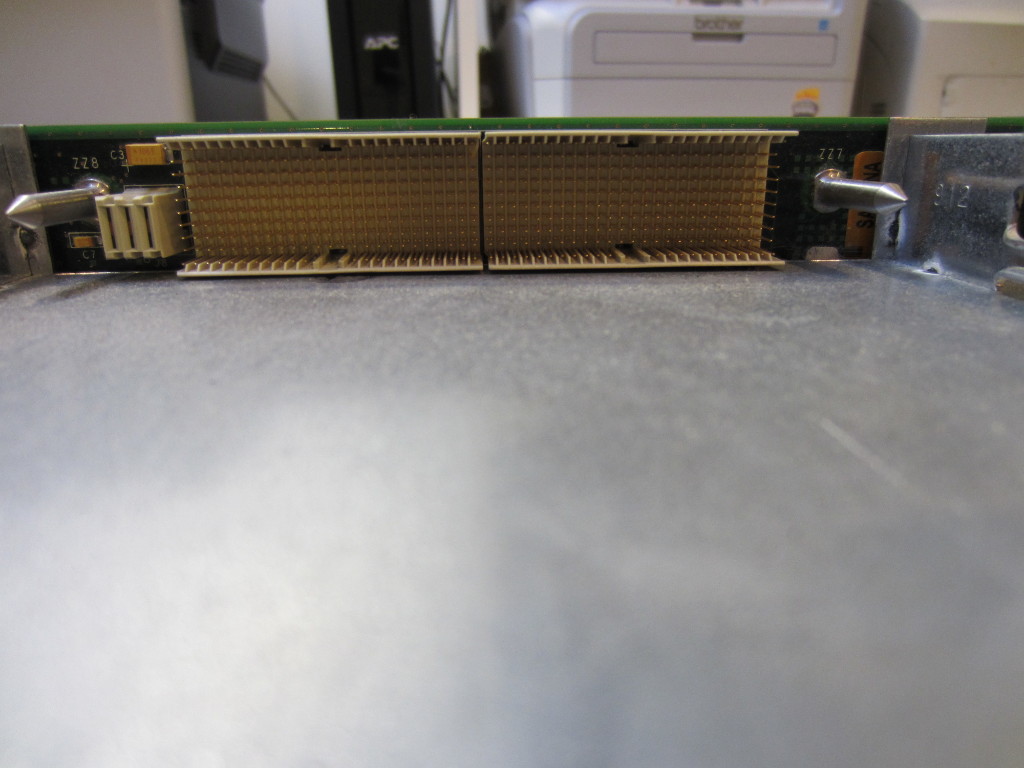
All modules are connected to the back plane via ERNI board-to-board IEC connectors. These modules can be easily removed by pushing the levels mounted on either side of the board and slid out. The picture on the right below shows the empty socket on the back plane after the module had been removed.
|
|
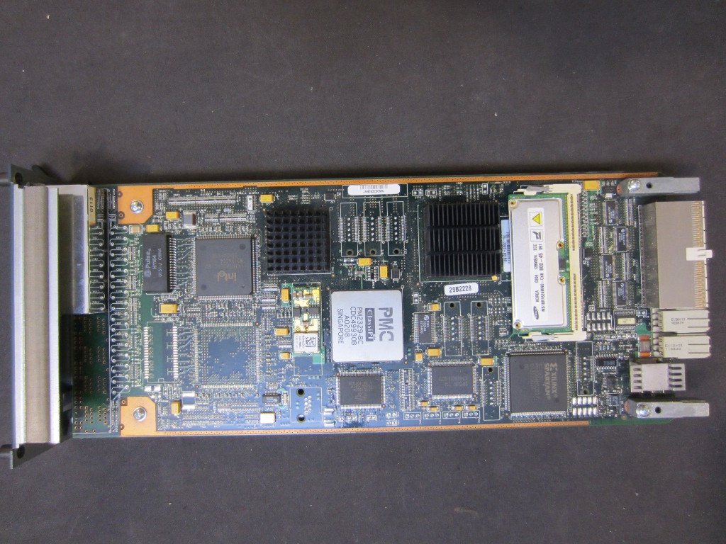
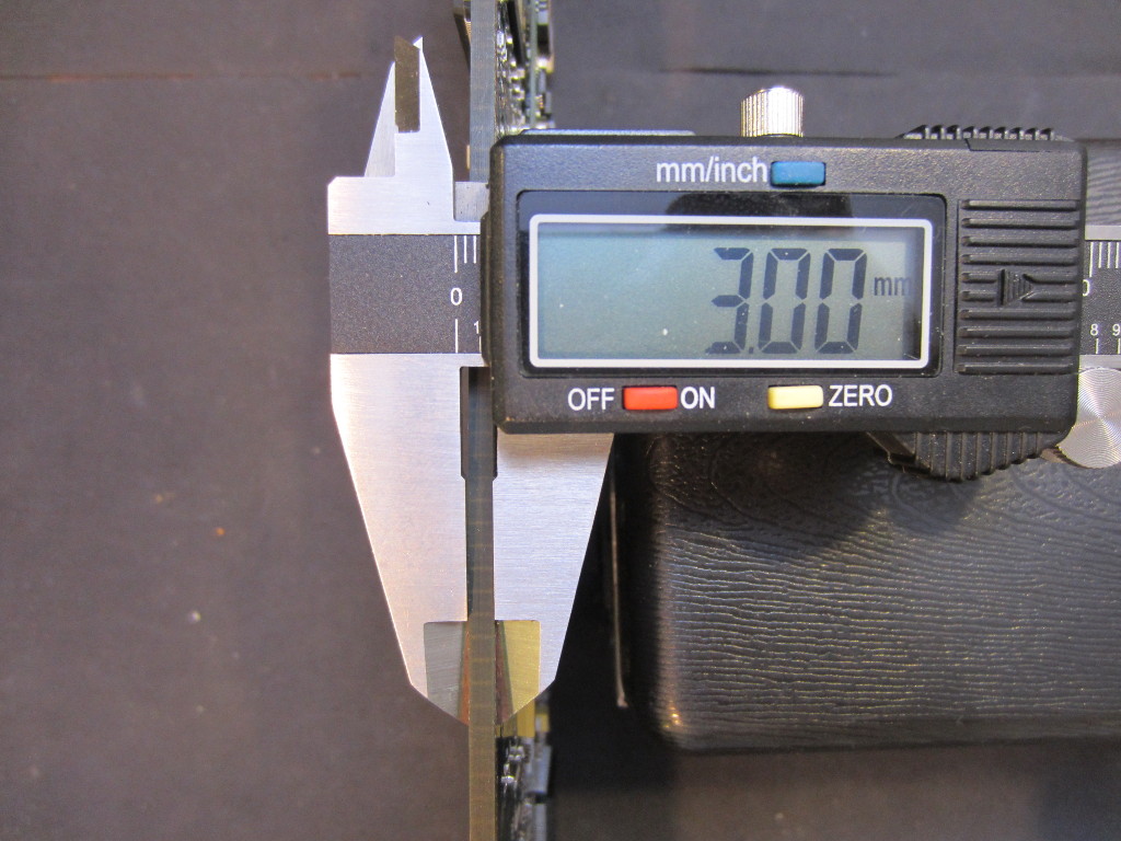
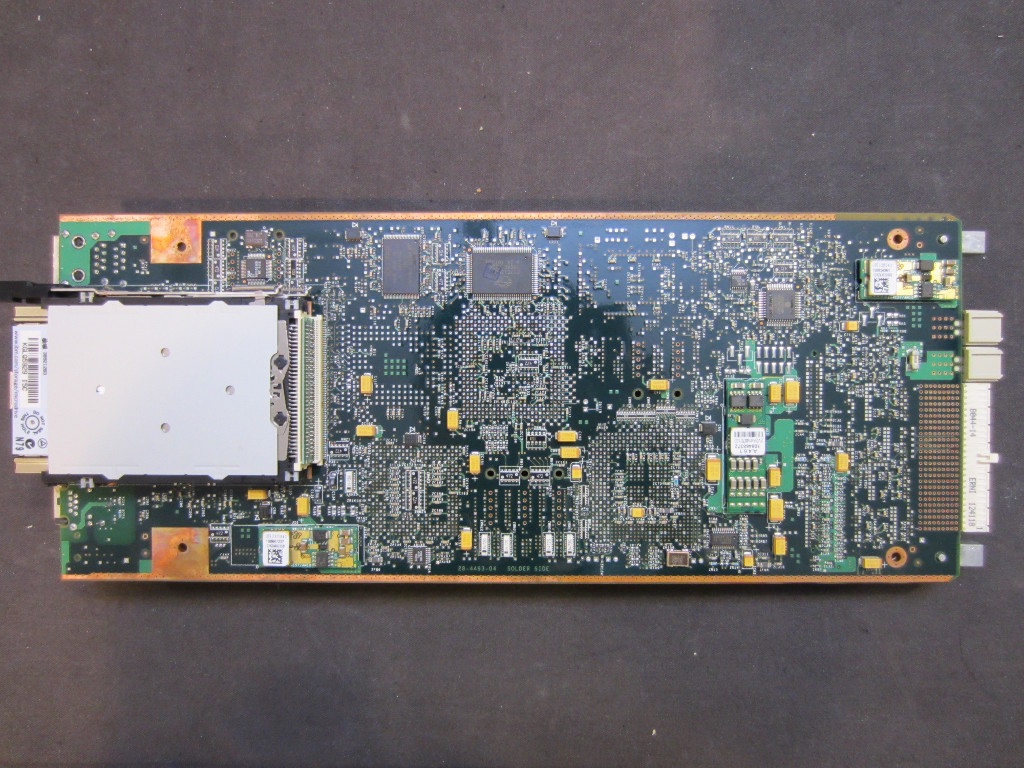
Like the internal mounted modules, all the plug-in modules are mounted using the same mechanism. The board shown below is the 8-port ethernet switch module. This module and the fiber channel module you will see later on were both assembled on 22-layer PCBs. I had seen boards with up to 18 layers before but this is the first time I actually saw a commercial product with a 22-layer board. The final PCB is quite thick (3 mm) due to the large number of inner layers.
|
|
The reason for this high layer count is partially due to the strict timing and signaling requirements of the two FPGAs (the ethernet module has only one FPGA but the fiber optics board has two). On the ethernet module we can see a PMC ClassiPi PM2329-BC packet content classification processor, a Xilinx Spartan II family FPGA XC2S30 and an Intel LXT9875 fast 8 port ethernet transceiver chip. We will take a look at those heatsinked chips a bit later.
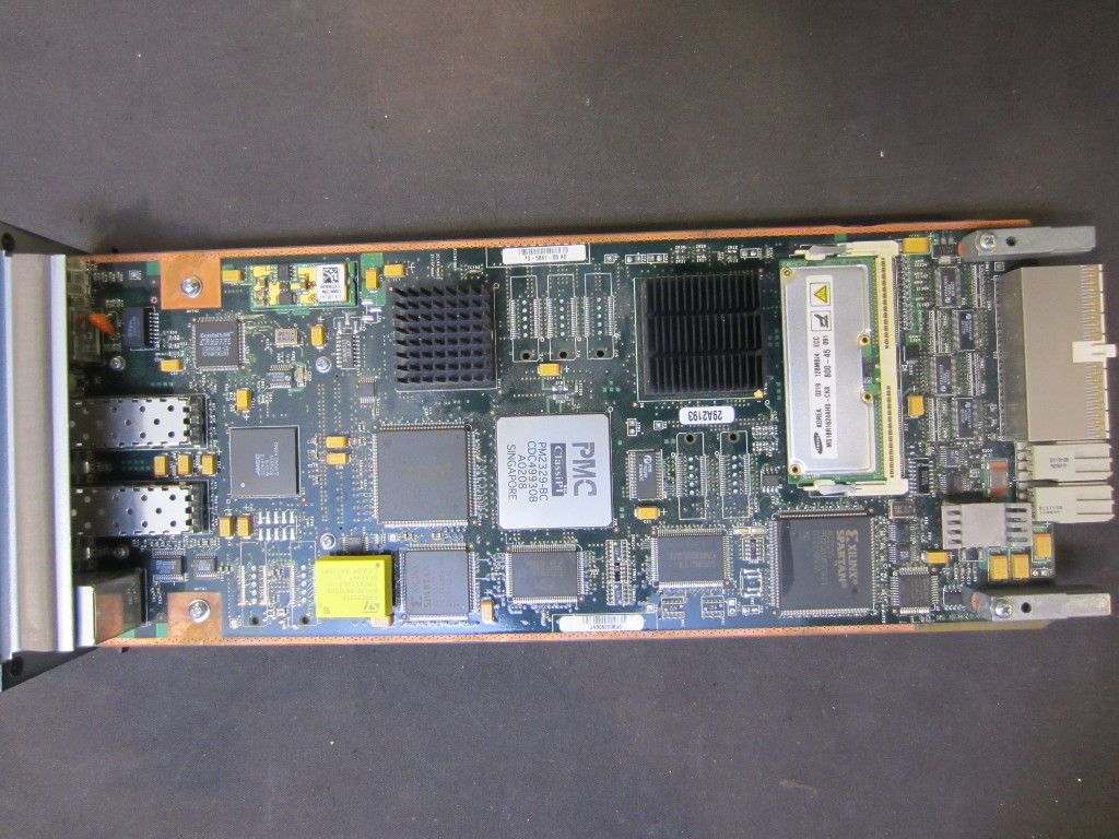
As you can see from the picture above, the board layout for the fiber optic module is largely identical to that of the network switch module. This board has two XC2S50 FPGAs and also has an Intel SPD6722QCCE ISA to PCMCIA controller. We will see the reason for this later.
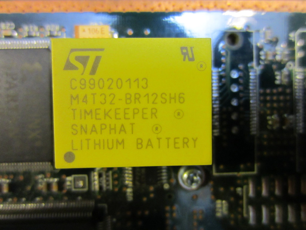
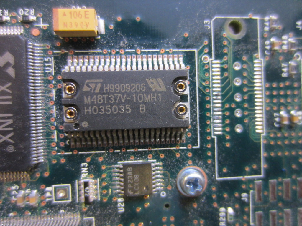
The fiber optic network board also has a realtime clock. The realtime clock chip M48T37V utilizes a SNAPHAT battery and crystal module which plugs in on top of the chip directly.
|
|
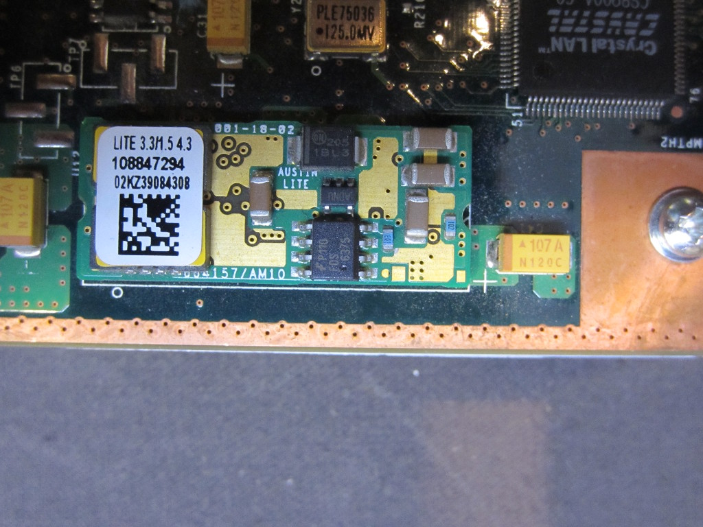
Each of the three boards shown so far has a heatsinked MOSFET. The PCB alone is not enough to handle the heat dissipation so a separate heat sink is added. Take a look at the heat sink, it does not make contact to the surface of the MOSFET directly. Rather, it is soldered onto the PCB and transfers the heat out directly from the metal tab of the TO-263 SUB75N03.
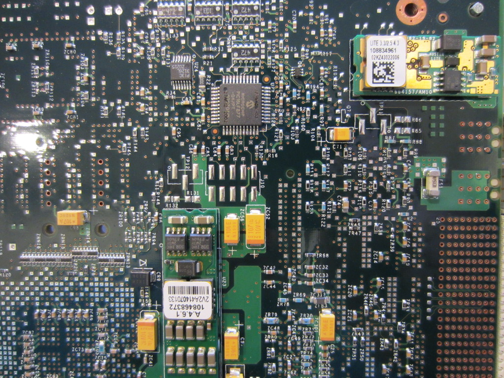
The image on the right below shows one of the many DC-DC converter modules which are used to provide the various voltages needed by the FPGAs.
|
|
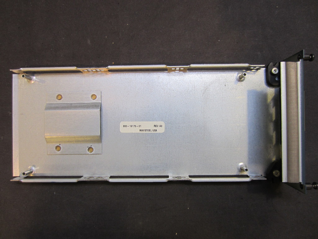
Here is a picture of the cradle after the board was removed. You can see the soft metal mesh on the edge of the cradle which guarantees the contact of the chassis after the module has been inserted to ensure good electromagnetic shielding.
The following are pictures of the underside of the fiber optic networking module. Two PCMCIA slots are available and hence the need for a ISA to PCMCIA bridge we saw earlier. In the closeup picture, we see a couple more DC-DC converters next to a PIC16FL877 microcontroller.
From the picture on the right below you can also see that the IEC connector is press-fitted not soldered. In fact most of the connectors inside this Cisco unit are press-fitted.
|
|
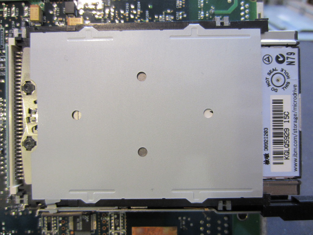
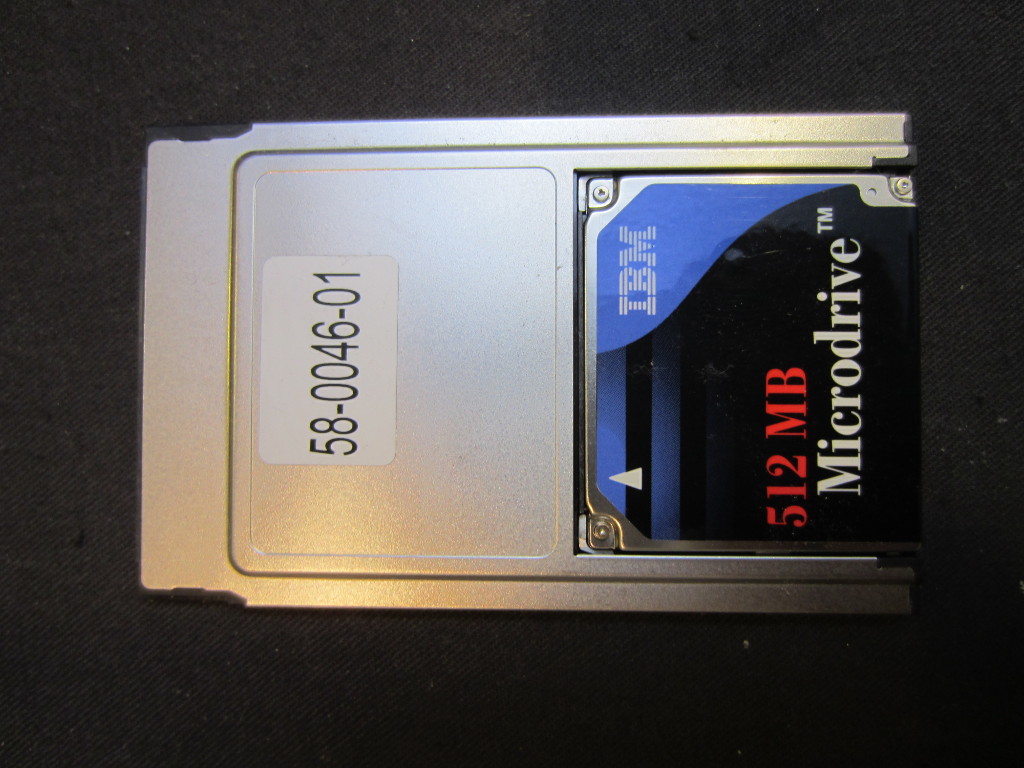
Here is a close look of the PCMCIA bays and the 512 MB IBM microdrive.
|
|
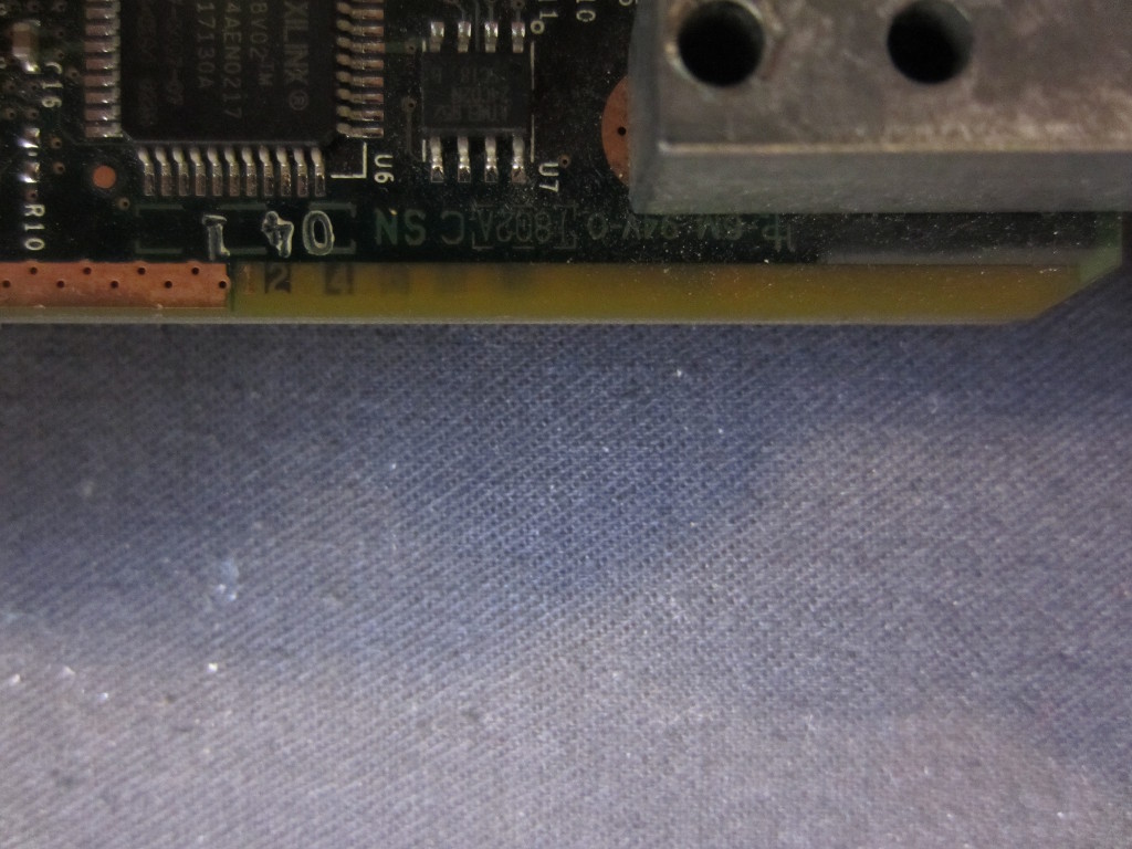
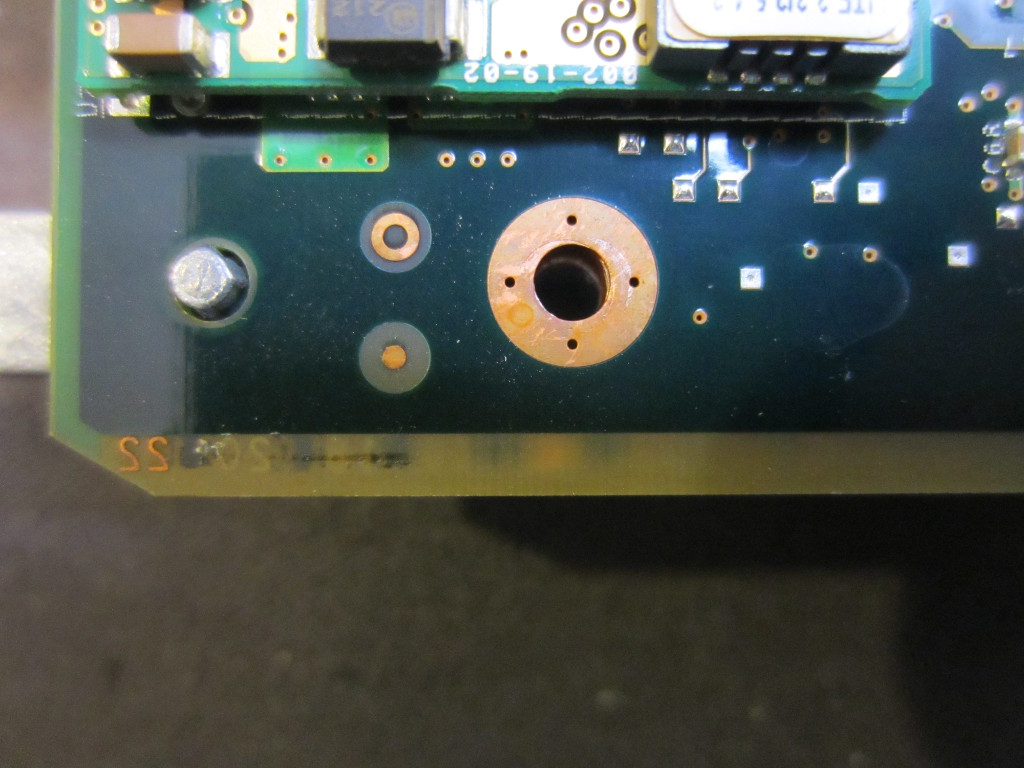
As I mentioned earlier, these boards are 22 layer PCBs. This can be verified by the markings towards the edge of the PCB as shown in the pictures below.
|
|
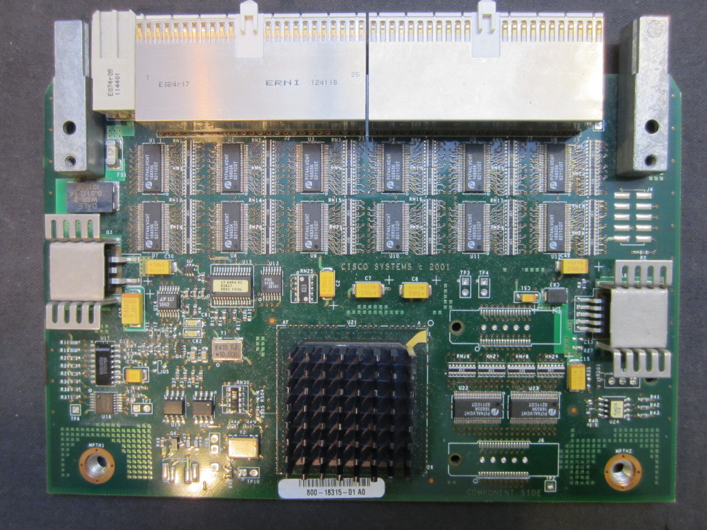
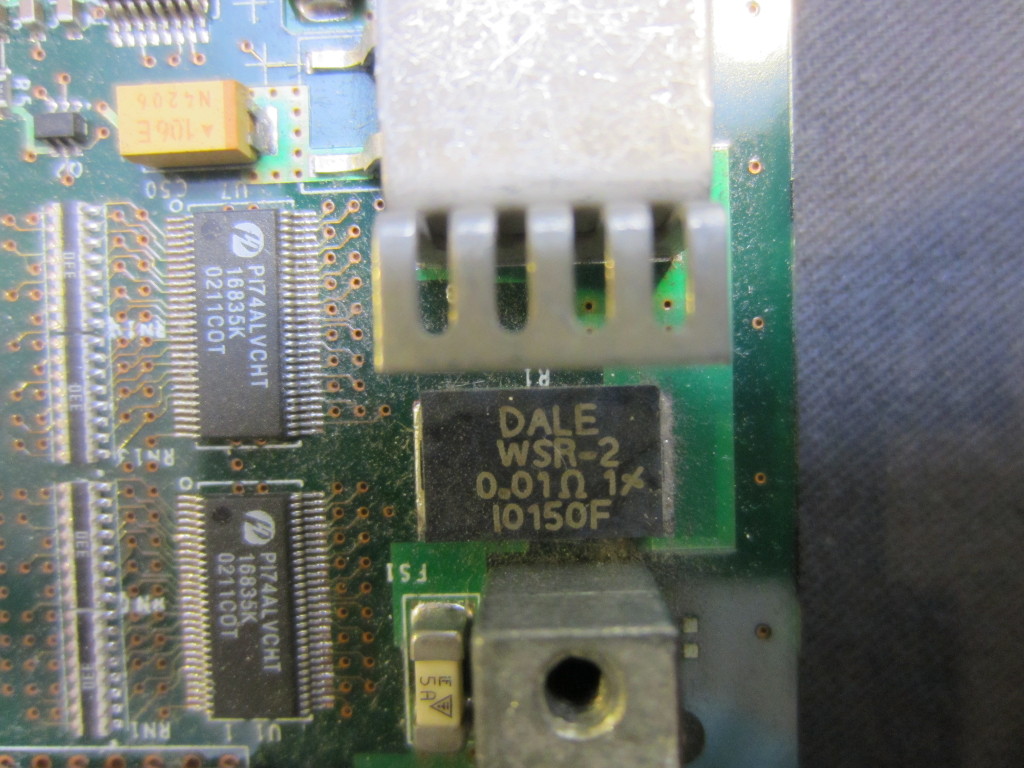
Again, here are a couple of pictures of the small interface board inside the unit after it was taken out of the chassis. This one is a 14 layer board. There is a 0.01 Ω current sensing resistor right next to the power MOSFET presumably for monitoring the current consumption.
|
|
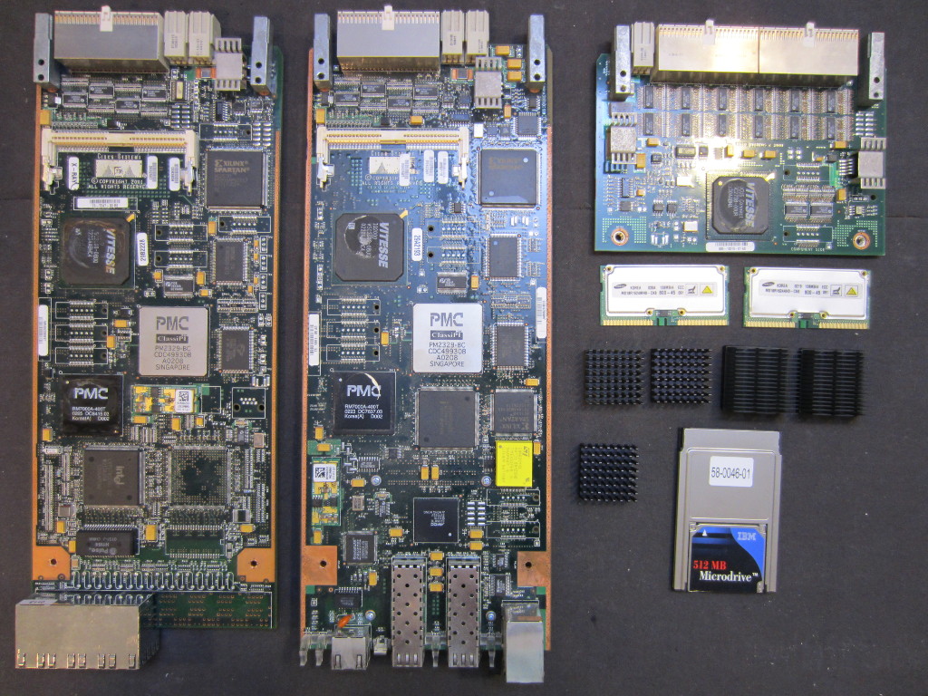
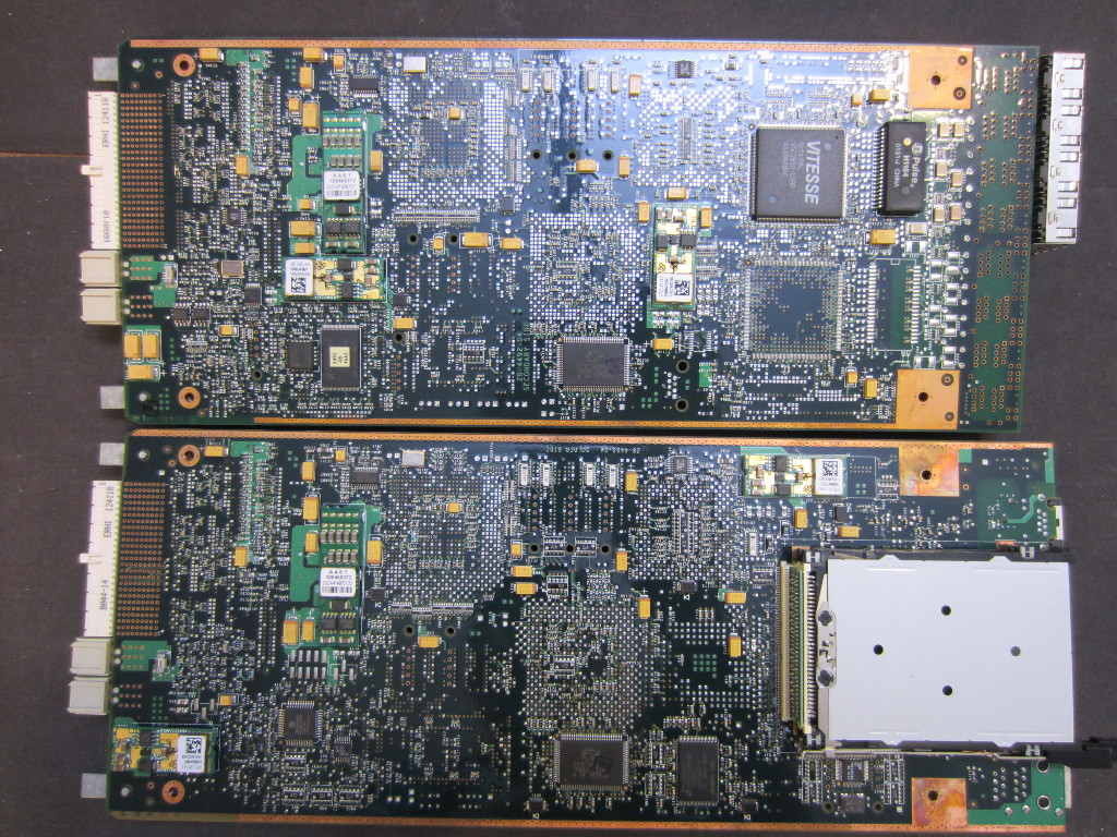
Here are a couple of pictures showing all the boards inside this Cisco switch. I had also removed all the heatsinks so we could see the other chips used. On each board, the two heatsinked ICs are a VITESSE VSC2100 packet processor (on the fiber optic board the processor is a VSC2102) and a PMC RM7000A-400T dual issue symmetric superscalar microprocessor. The chip on the smaller PCB is a VSC2708 8 port switch.
Because these modules were designed to be hot-swappable, there is a LTC1642 hot swap controller on each of the board.
|
|
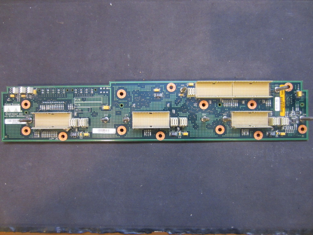
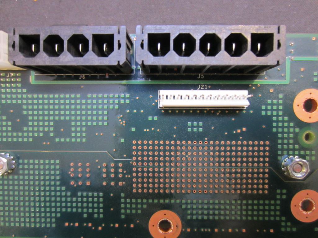
These two are pictures of the back plane. Almost all the connectors are press-fitted. The picture to the right shows the 3.3V power input connectors. Due to the current capacity needed, all pins within each connectors are shorted together.
|
|
Finally, let’s take a closer look at the switching power supply used here. This is power supply was sourced from ASTEC, it can provide 80A on its 3.3V rail!
|
|
So if nothing else, this switching power supply can definitely be used in another project.

