Monochromator is one of those things that has always fascinated me. Over the years, I have done quite a few experiments (I, II, III) with an EP200Mmd monochromator and it was a lot of fun. Because monochromators are such highly specialized equipment, decent ones are hard to come by at reasonable prices second hand. So my strategy has been to scour eBay once a while and pick up bit and pieces whenever I can.
Among the stuff I have picked up over the years is a SPEX HS1000 (now HORIBA Jobin Yvon) HandScan/KeyLink controller which is used for controlling many of the SPEX/Jobin Yvon monochromators and spectrometers. Hopefully one of these days, I would be able to get a supporting model and put this controller to use. But for now, let us take a look to see what is inside of this rather large controller unit.
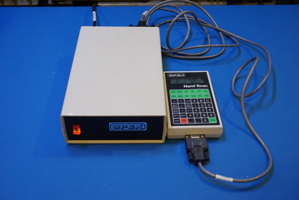
The HS1000 comes with a base controller box and a keypad that is connected via a 9 pin RS232 cable.
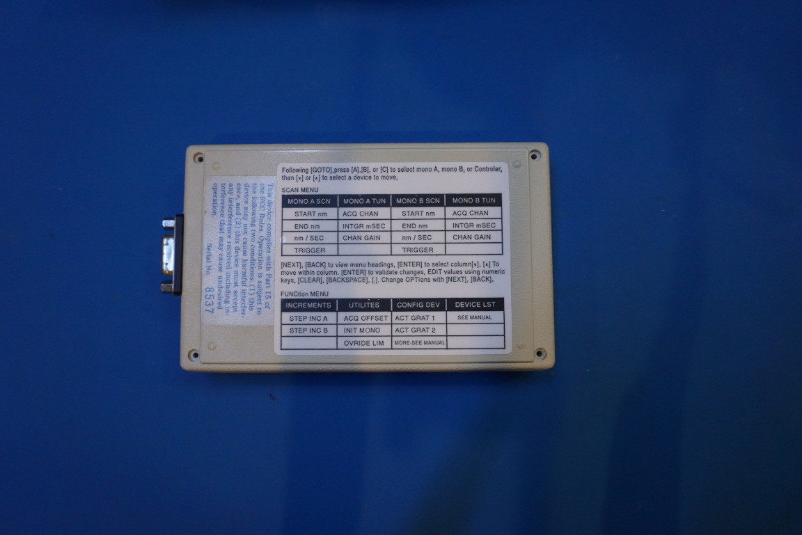
At the back of the keypad box, there are some handy instructions on how to operate the controller.
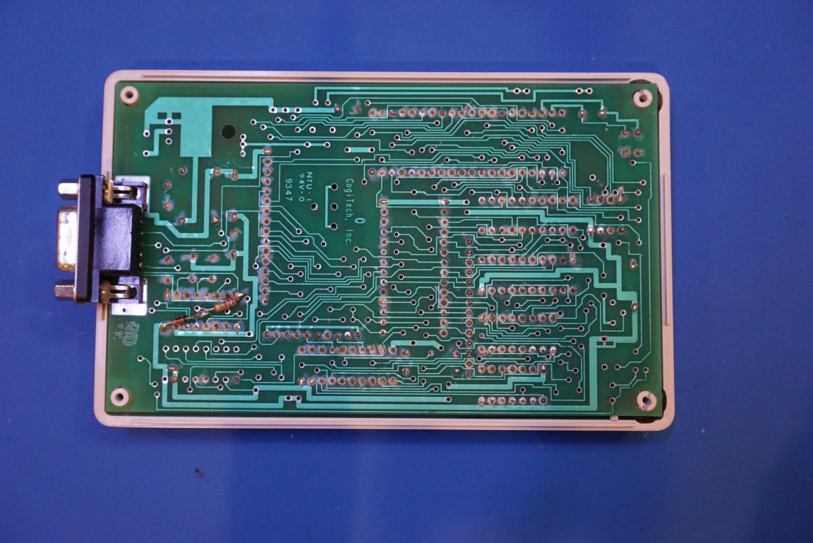
Here is a picture showing the bottom of the PCB inside the controller box, some minor bodges can be seen here.
It took some persuasion to pull out the PCB as the LCD is glued onto the case. Here are a couple of pictures showing the other side of the board.
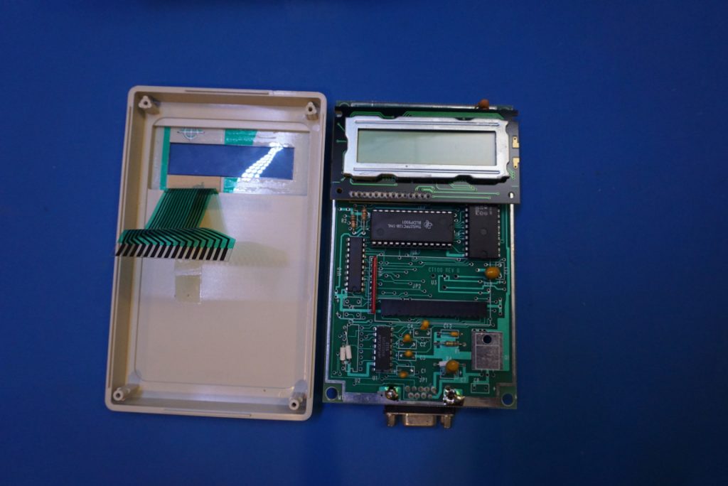
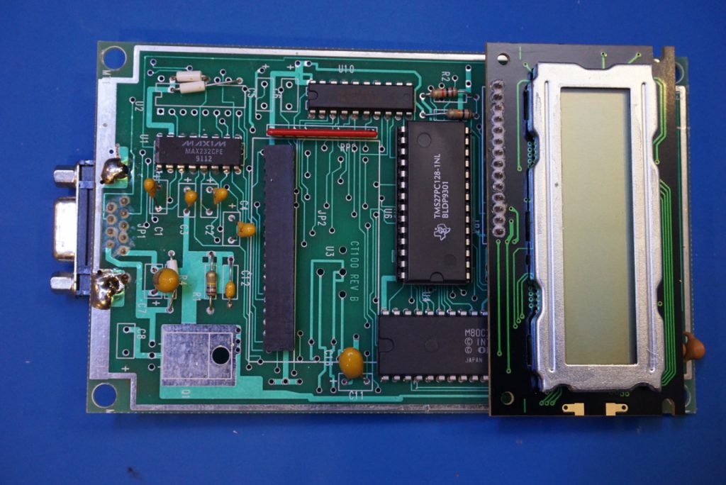
At the heart is a 80C31 ROM-less 8051 microprocessor. The instructions are stored in the adjacent 128 kbit one time programmable (OTP) ROM. The RS232 communication is handled by the venerable MAX232.
The keypad is powered by the RS232 cable (via pin 9, ring indicator), but the board also has footprint for a three terminal regulator so presumably, this board is also used in a version where it can be separately powered.
Opening up the main controller box reveals the circuitry inside. There are two boards vertically stacked together.
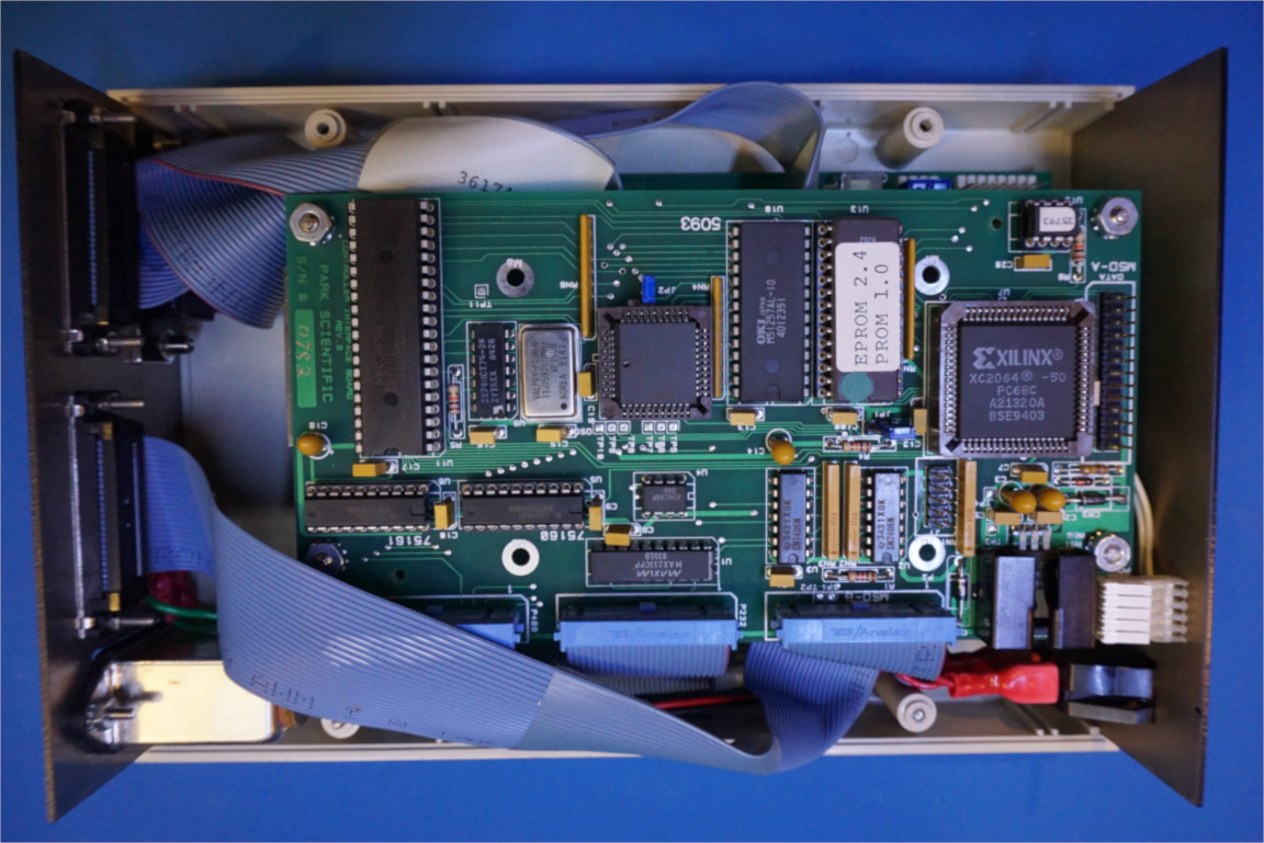
Here is a another picture of the top board:
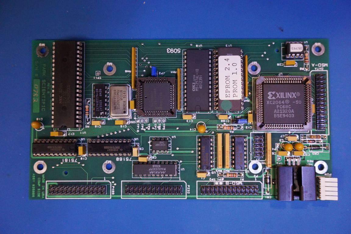
The microprocessor on this board (top center) is an 8051. Interesting enough, an additional FPGA (Xilinx XC2064) is also used. Although XC2064 is classified as a logic cell array chip, it is the world’s first FPGA ever used commercially.
The GPIB logic is handled by an NEC UPD7210C IEEE-488 controller. As usual, the serial communication is done via an MAX232 chip.
On the bottom PCB, there is more digital logic on the right half of the board.
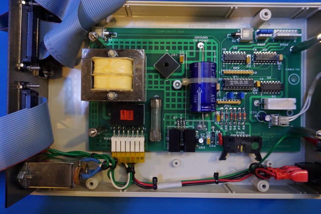
There is a small TIBPAL16R4 high-performance programmable array logic chip and I am not entirely sure what it is used for here. There are a couple of unused headers on this board (P100, P300), perhaps they are used for programming the PAL? By the look of it though, this digital circuitry interacts very little with the main board that is mounted on the top.
I am also curious about what the two momentary switches S1 and S2 are for. Since they are located at the bottom of the two stacked PCBs, I can only assume they were perhaps used for functional testing during the assembly process.
To fully test the functionality of this controller unit, I would need to find a compatible monochromator/spectrometer to hook up to. And that is something on my to-do list.
You can check out the video of this teardown below:

