I just picked up a LogiMetrics A300/S 2 GHz to 4 GHz (S band) traveling wave tube amplifier (TWTA) on eBay. I had done an extreme teardown of an HP 493A TWTA a while ago and it was quite fascinating to see what’s inside of a TWT. This LogiMetrics A300/S was made from the late 70’s and unlike the HP 493A it was made entirely using solid state devices (e.g. transistors and ICs), the TWT itself of course remains a vacuum tube.
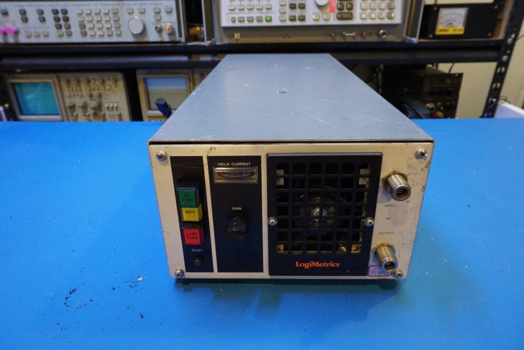
This unit is in non-working condition and as you can see from the picture above, it is conveniently missing the fuse cover as well. It also seems to have a stuck resettable relay. Unfortunately, the schematics for this LogiMetrics A300/S is no where to be found so fixing it could be challenging. For this blog post though, we are going to just open it up and take a look at what is inside.
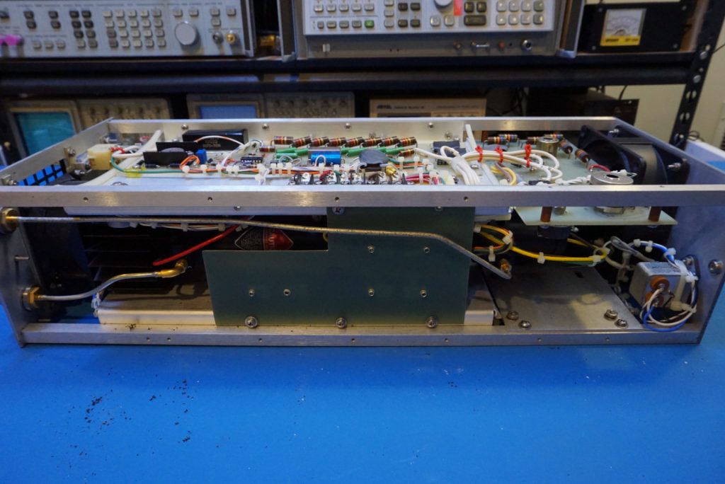
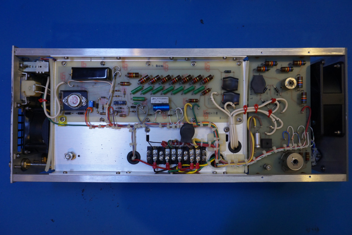
Here are a couple of pictures showing the A300/S with the case removed. As you can see there are circuit boards mounted on pretty much all sides as well as inside, making disassembly and repair more challenging.
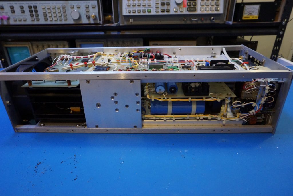
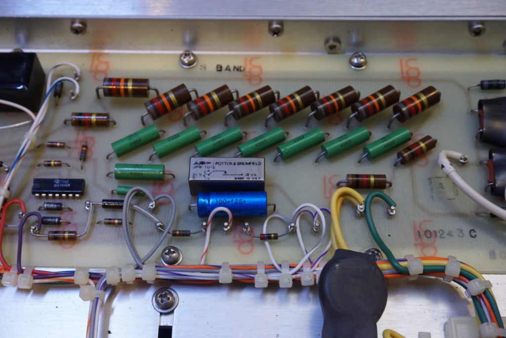
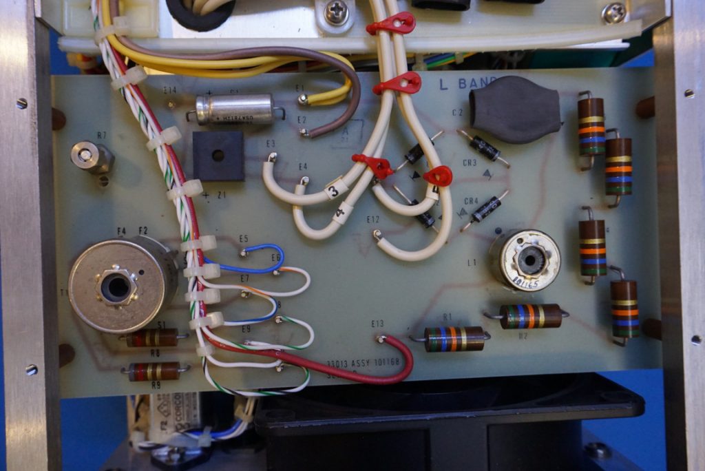
There are two circuit boards mounted on the top side. Judging from the components and layout, these are presumably handling the voltages to the TWT. The connections to the TWT are made at the terminal block towards the middle bottom.
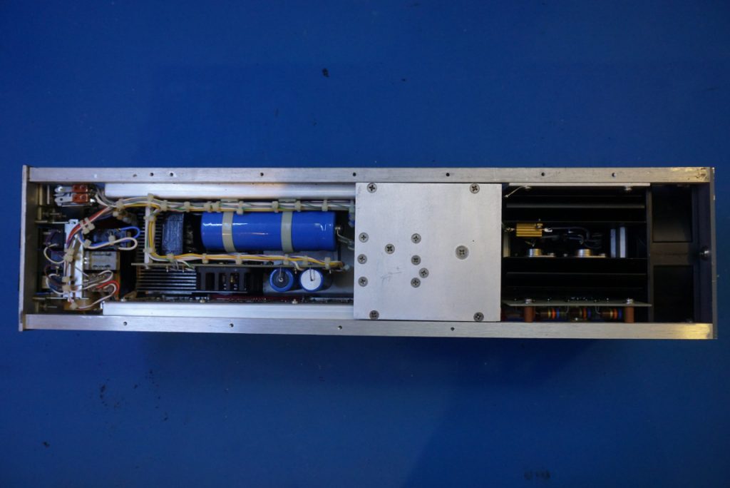
The picture below to the left shows what looks like the high voltage portion of the circuitry. And the picture to the right seems to another rectification and filtering board.
Notice how some components and wires are soldered on standoffs rather than onto the PCB itself.
Towards the left below is a picture showing one side of the TWTA. You can see some large filtering capacitors and power transistors tucked inside. After removing the screws on the center metal plate, it revealed that there were just a large choke, a high voltage diode (MR832) and a bridge rectifier on this plate.
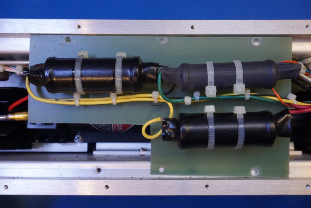
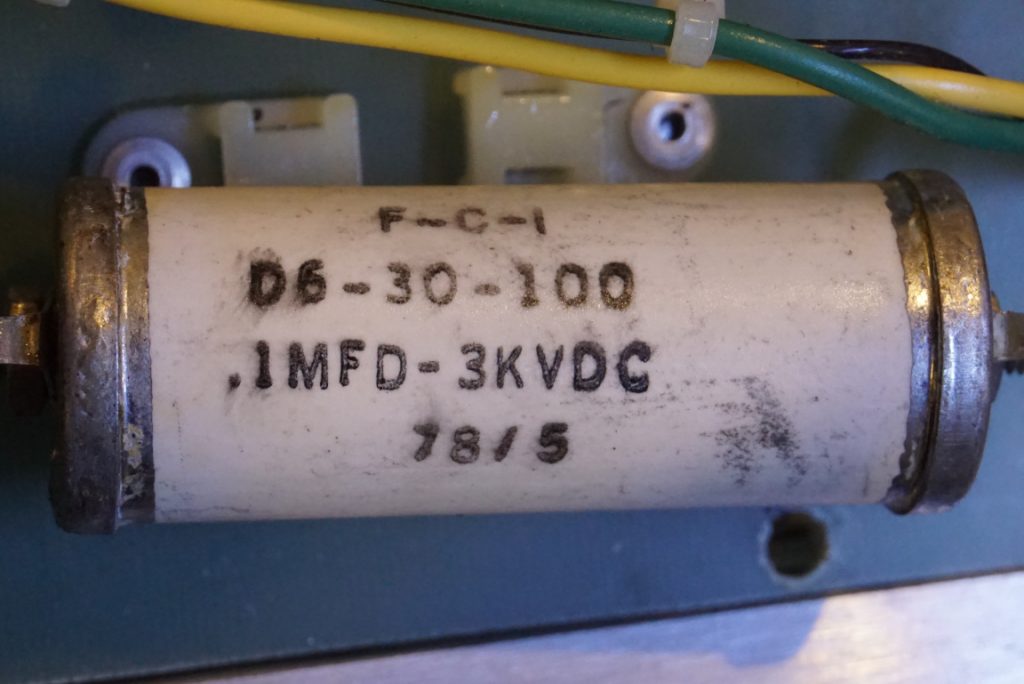
And as it turned out, the other “L” shaped PCB vertically mounted on the other side of the chassis holds only three capacitors. I cut open the insulating wrap on one of the capacitors and as you can see that one is a 100nF 3kV high voltage capacitor. I assume the other two are also high voltage capacitors.
After the capacitor board moved out of the way, you can see the traveling wave tube inside the unit:
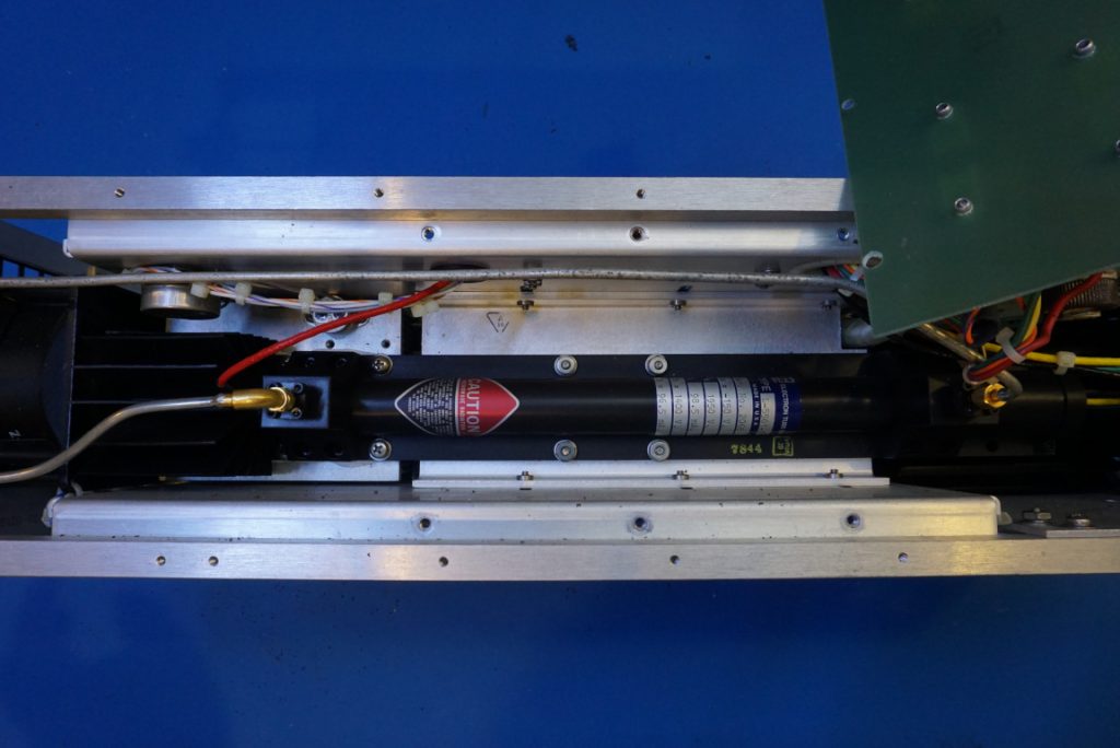
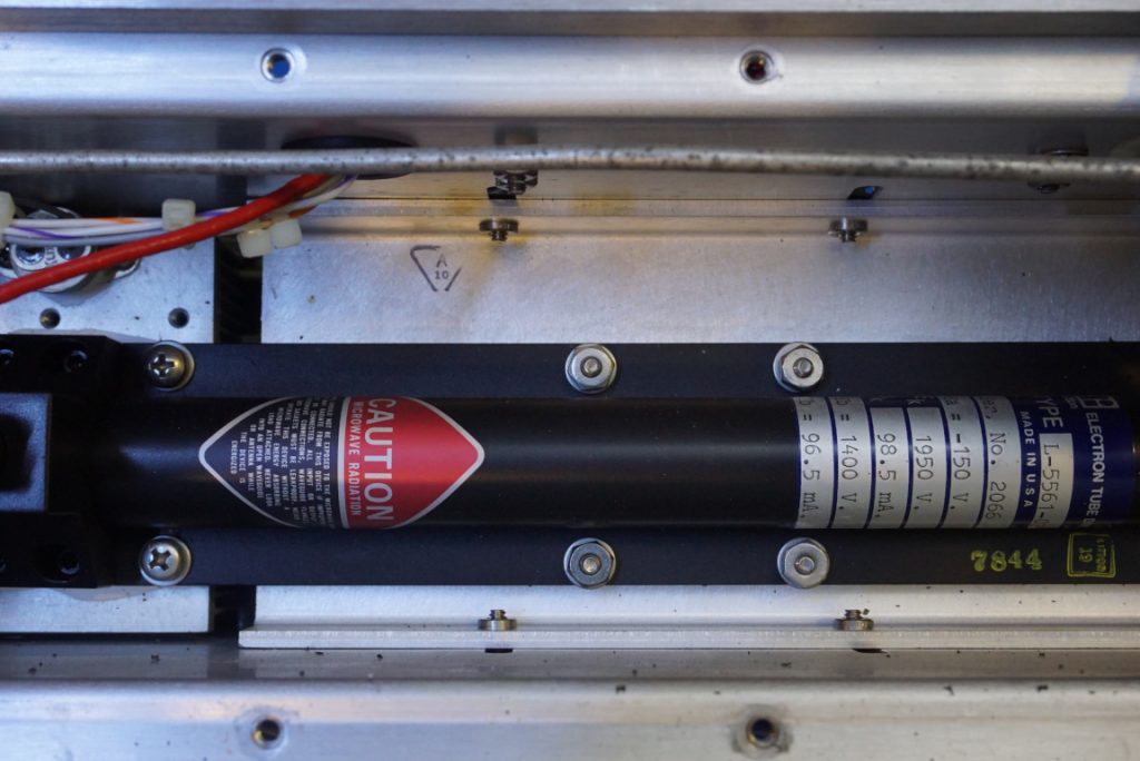
The TWT is a Litton L-5561-02 tube, although I could not find any detailed information on the internet. According to the label on the tube, the parameters are specified as follows:
- Ea = -150 V
- Ek = 1950 V
- Ik = 98.5 mA
- Eb = 1400 V
- Ib = 96.5 mA
These TWTs were clearly not mass produced. This is evidenced by the rather low serial number: 2066.
Because this TWT is capable of outputting 20 Watts of RF power, you can see the massive heatsink around the anode section. The heat is generated by the bombardment of the high energy electrons.
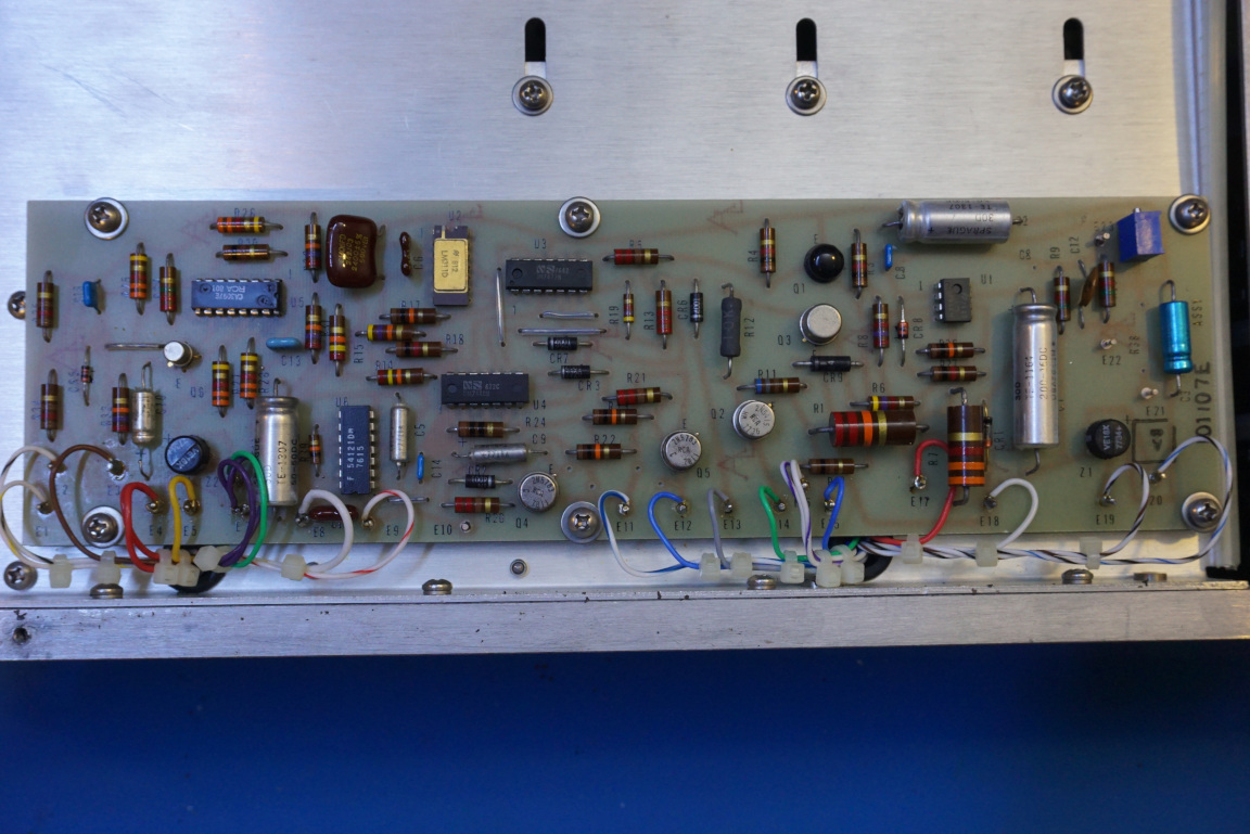
Mounted on the bottom side is the main PCB. It is interesting to see a CA3097E thyristor/transistor array chip there. I am not entirely sure what it is used for here however. The electrolytic capacitors on this board are all showing some signs of leakage and degradation. So any future repair will likely start here.
The teardown video of this LogiMetrics A300/S TWTA is linked below:

