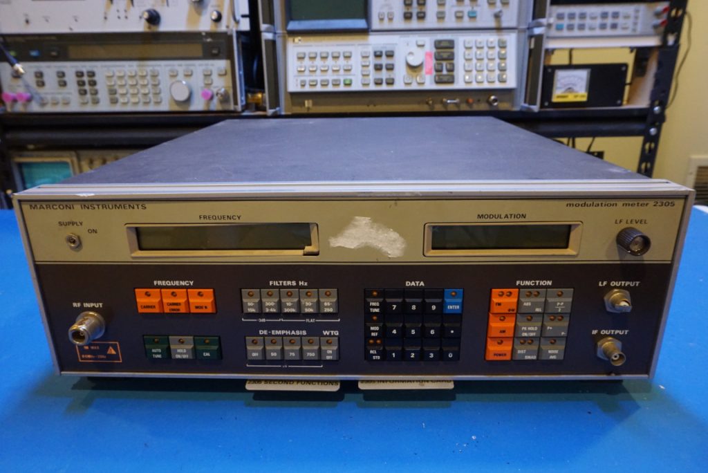
I picked up a Marconi 2305 modulation meter off eBay the other day. As the name indicated, a modulation meter is used to measure the modulation characteristics of a source signal. The Marconi 2305 is capable of measuring amplitude/frequency and phase modulated signals from a few hundred kHz all the way up to 2 GHz.
The Marconi 2305 was built sometime between the late 70’s and 80’s. It is a pity that the iconic British Marconi Instruments went under in 1998 and had since changed hands a couple of times.
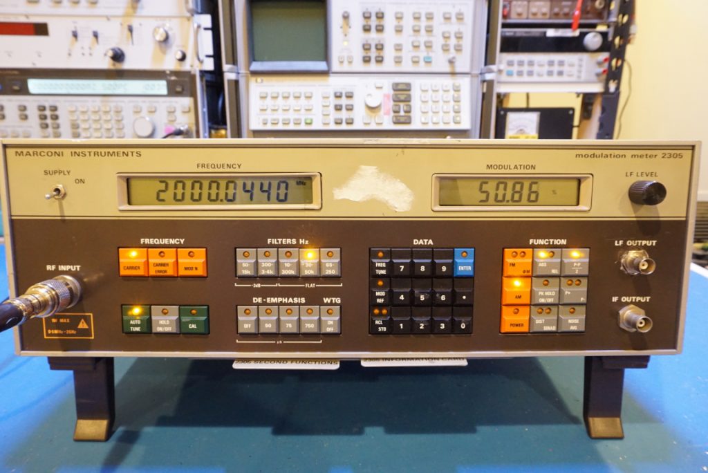
The instrument arrived with a damaged BNC connector, a snapped off power switch and some other cosmetic issues. As you can see in the pictures below, I was able to restore it to its original glory. I even managed to 3D-print an end cap for the LF level adjust knob.
It is amazing to think about how much technology has evolved. At its core, the entire instrument is really just a glorified superheterodyne receiver along with some measurement circuitry. All the core and supporting circuitry would probably fit into a single FPGA nowadays and the receiver itself would have been made entirely digital. But back in the days, the only way to build an instrument like this is through some cleaver analog circuit design and RF engineering.
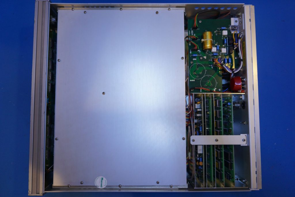
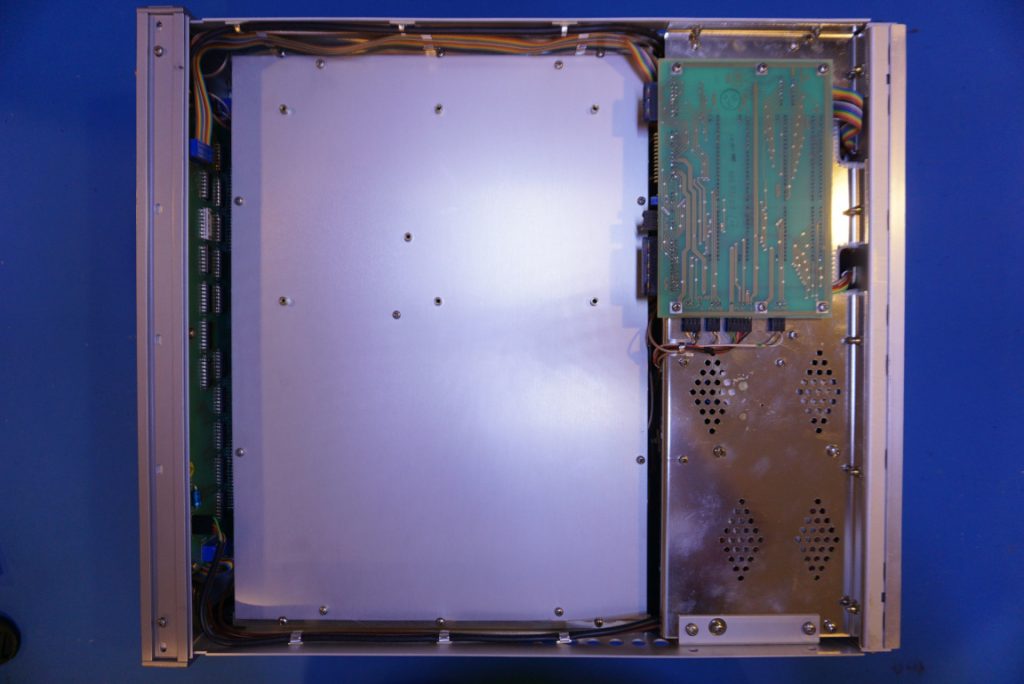
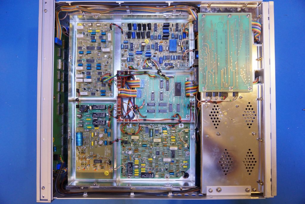
As you can see in the pictures below — after the top cover and the RF shielding have been removed — that the Marconi 2035 is indeed a piece of art. Besides the obvious power supply portion to the upper right corner, the entire chassis is filled with circuit boards. Remind you that this is only the top side, and the bottom side of the unit is equally densely populated as well.
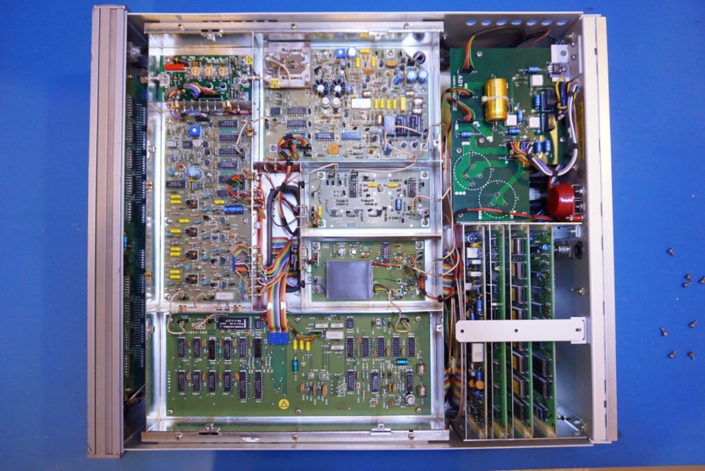
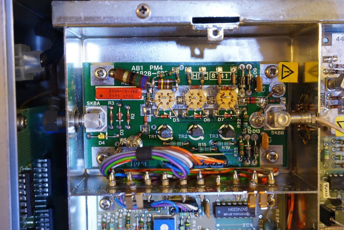
The RF section is divided into several self-contained building blocks and each is enclosed in its own shielding enclosure. The picture below shows the AB1 attenuator board. Each of those gold-colored multi-pin components is a RF relay used to switch in different attenuation. Notice how power is passed through between adjacent RF enclosures. Feed-through capacitors are used to ensure that any electronic noise is sufficiently filtered and isolated.
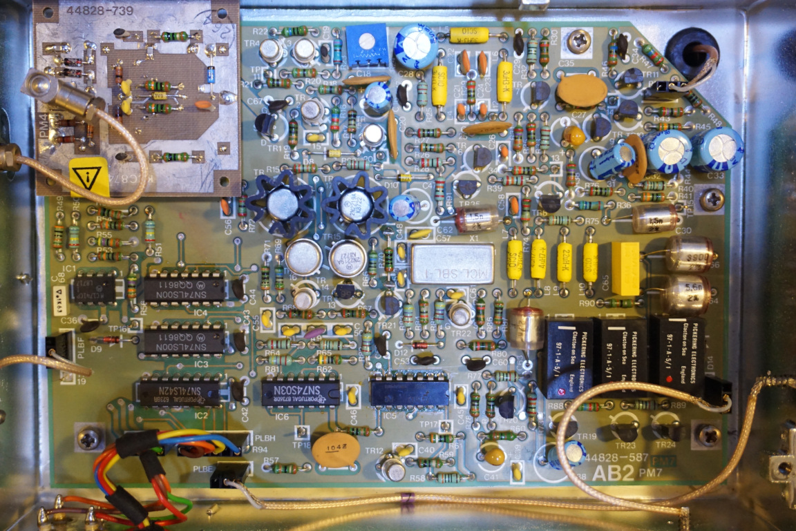
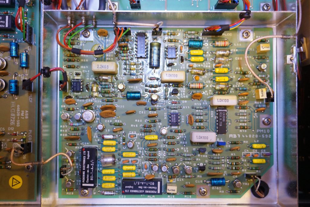
After the signal passes through the attenuator, it enters the sampling gate and the mixer board. The sampling gate is used to produce an IF in conjunction with the local oscillator (LO). The mixer used here is essentially a step recovery diode based harmonic mixer.
The picture below shows the voltage-controlled oscillator board. There are actually multiple VCOs (to be precise, there are four VCOs here) and each is used to tune in its specific frequency range. The datecodes on the various ICs suggest that this unit was built in late 1988.
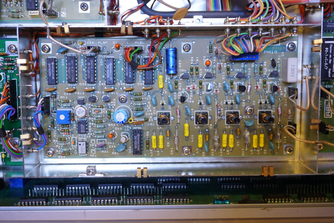
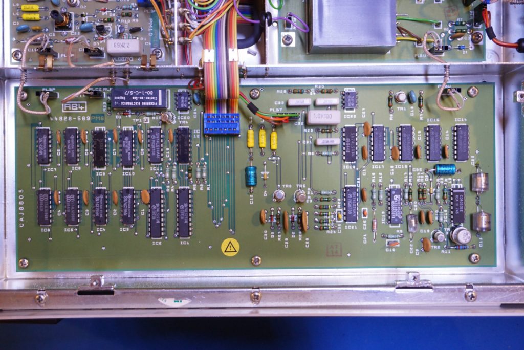
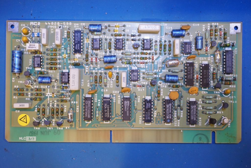
The picture to the left below is the counter limiter board and the picture to the right is the programmable divider board. The counter limiter is nothing but a level translator. It is used to covert the IF signal to be TTL compatible.
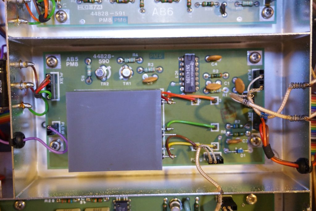
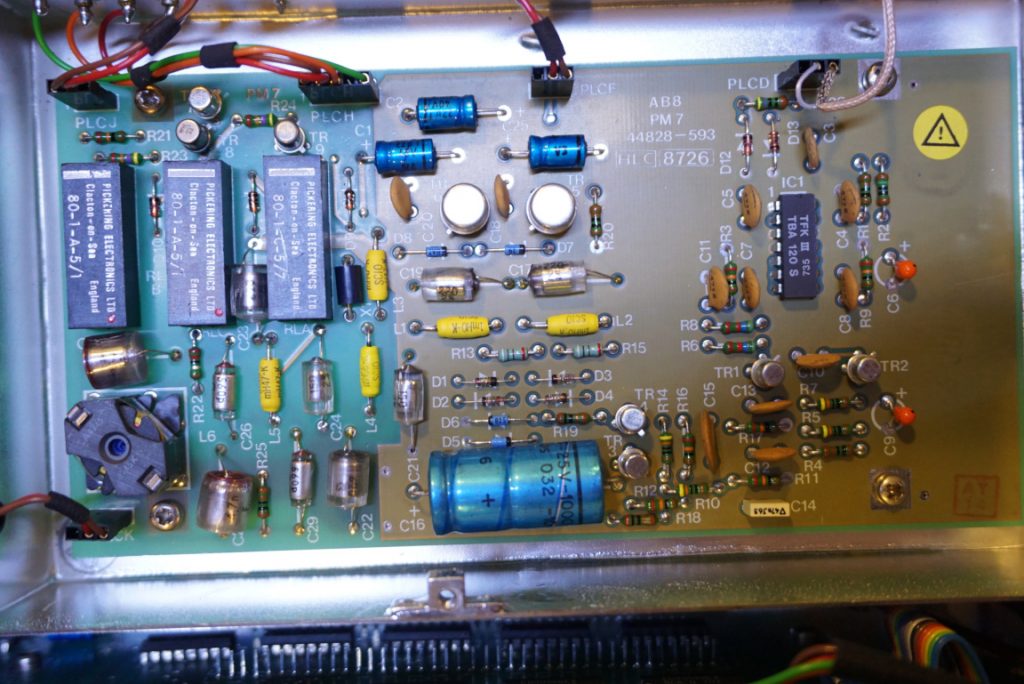
Here is a picture of the reference oscillator board. The reference oscillator is oven controlled to ensure the maximum stability.
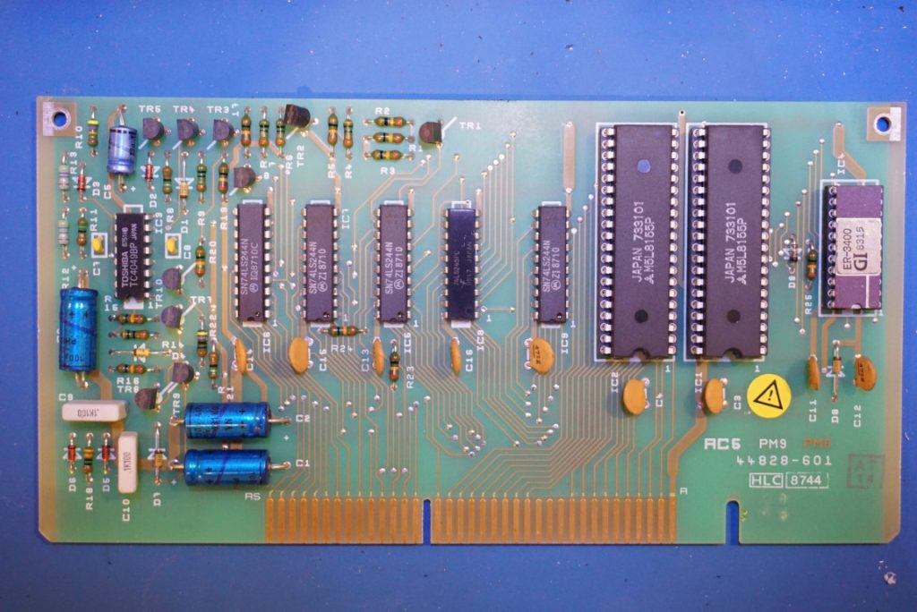
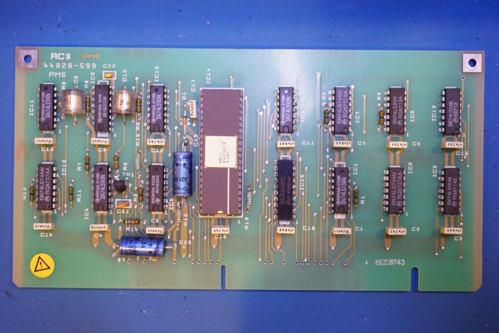
The digital boards are vertically plugged into a back plane. There are two processor boards in this unit. The two M5L8155P‘s on the board to the left are SRAMs and the ER3400 is an electronically alterable readonly memory chip (EAROM).
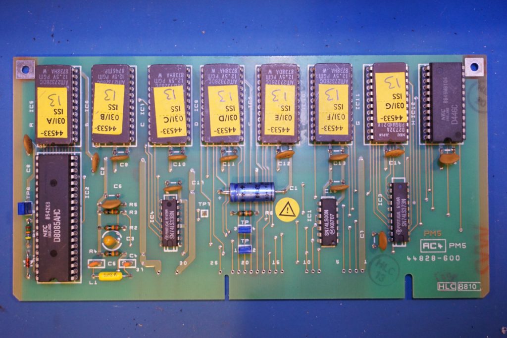
The board to the right blow is the main processor board. The microprocessor used here is an NEC D8085AHC 8-bit processor. Altogether 7 4 k EPROMs are used to store the program instructions. The NEC uPD446C is a 2 k SRAM chip.
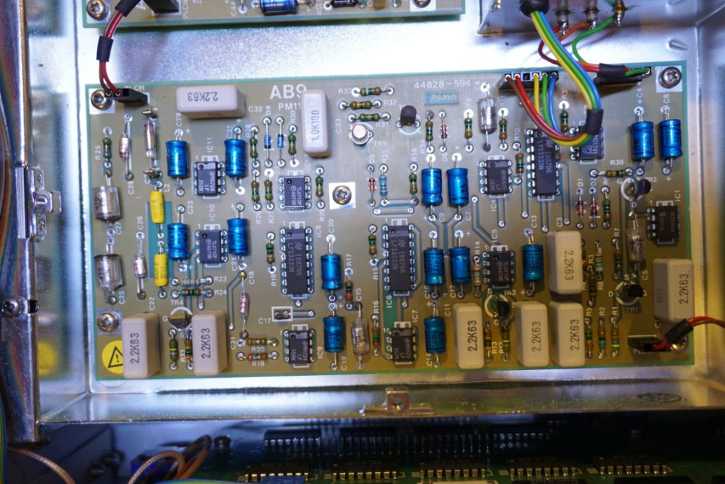
The remaining two digital boards are a voltmeter board (left below) and a counter board. The counter board utilizes a custom IC. Care needs to be taken when dealing with this board as the custom chip is unobtanium nowadays.
Flipping over the chassis reveals the remaining RF circuitry.
Here are the AM and FM detector boards respectively. The AM detector board detects the modulation depth of the AM signal and the FM detector board measures the frequency and phase deviation depending on whether the signal is frequency modulated or phase modulated. The service manual is a good place to read for a good understanding of the principle of operations.
The LF amplifier portion (to the left below) is responsible for amplifying the demodulated audio signal. The board in the picture to the right below is the LF filter board.
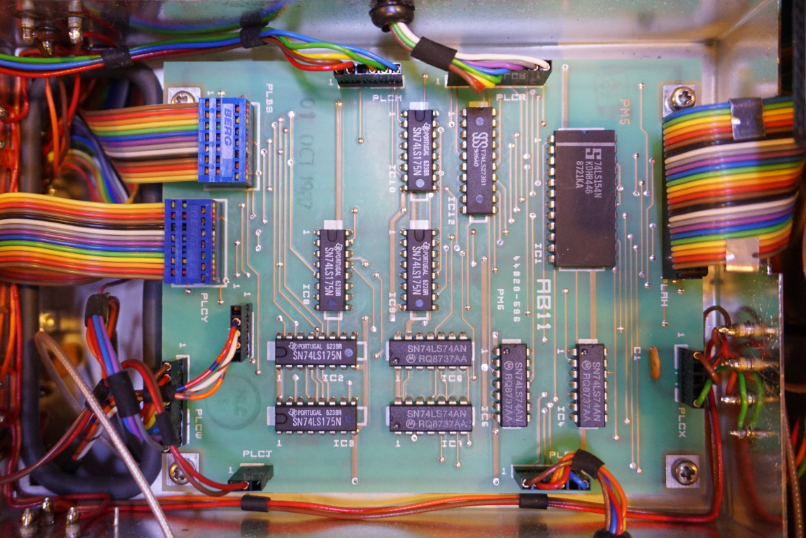
Finally, there is the AB11 latch board that routes the signal among the other portions of the subsystems.
Consider the among of engineering that went into this Marconi 2305, I couldn’t help but wonder what the original cost of this instrument must be!
A video of this teardown is linked below:
And here is a video detailing each of the modulation measurements:

