Electrophoresis power supplies are commonly found in biology and other life sciences laboratories. These power supplies are usually capable of supplying high voltages and high currents required for gel electrophoresis–a method used for separating DNA, RNA and other protein fragments based on their size and charge. There are many used electrophoresis power supplies out there in the second hand market and can be bought quite cheaply. I am curious whether these electrophoresis power supplies are suitable for electronics lab use as a lab grade high voltage power supply can be quite expensive. So I recently picked up one from eBay to take a look.
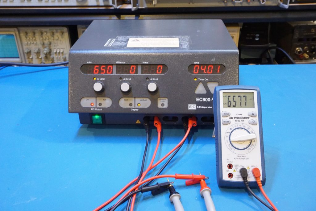
The electrophoresis power supply I bought is an EC600-90, a 4000V/300mA/300W high voltage power supply. It was made by E-C Apparatus Corporation in the mid 90’s. E-C was later acquired by Thermo Fisher Scientific.
From the get go, it became apparent that this power supply was built specifically for electrophoresis and nothing else. When the output is enabled, the power supply slowly ramps up its output voltage and it takes ten to fifteen seconds before the output reaches the preset value. The slow settle time alone would make it useless in situations where the load is dynamic and changes rapidly or has transient nature. But for steady resistive load or slow varying load, this kind of power supply should handle just fine.
The second issue is that there is a safety feature builtin which disables the output when no load is detected. Although only a few microamps are required to prevent the load detection circuit from tripping, it is very inconvenient to have to connect a resistor to the output as if the resistor is too large it may not pass sufficient current to defeat the load detector at low voltage settings. But if the resistor is too small, it will generate a lot of heat. A 3MΩ resistor is the largest I could use for the entire range of this power supply, but at 4000V it would require a 5W resistor. So for this power supply to be useful in a lab setting the no load detection has to be disabled. I will come back to this shortly.
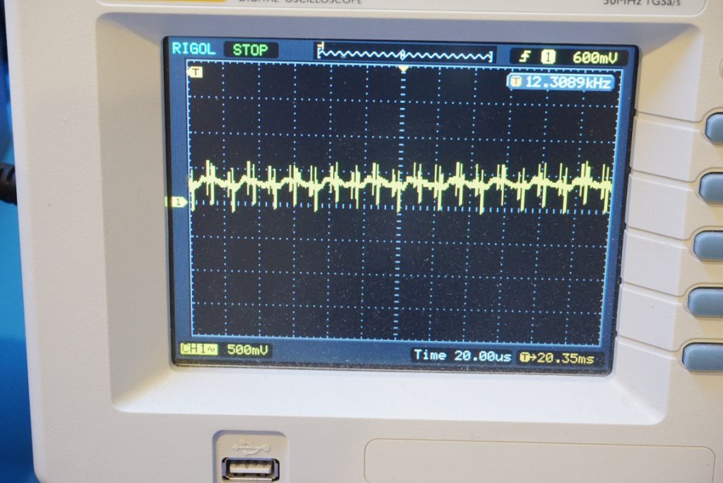
A third problem with this power supply is the excessive ripple. In operation, the ripple is roughly 500mV (see screenshot below). Although the ripple does not change much across the entire voltage range, it is too high for many electronics applications.
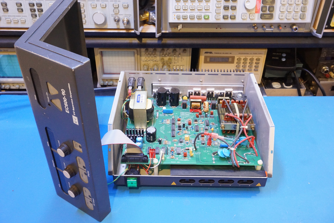
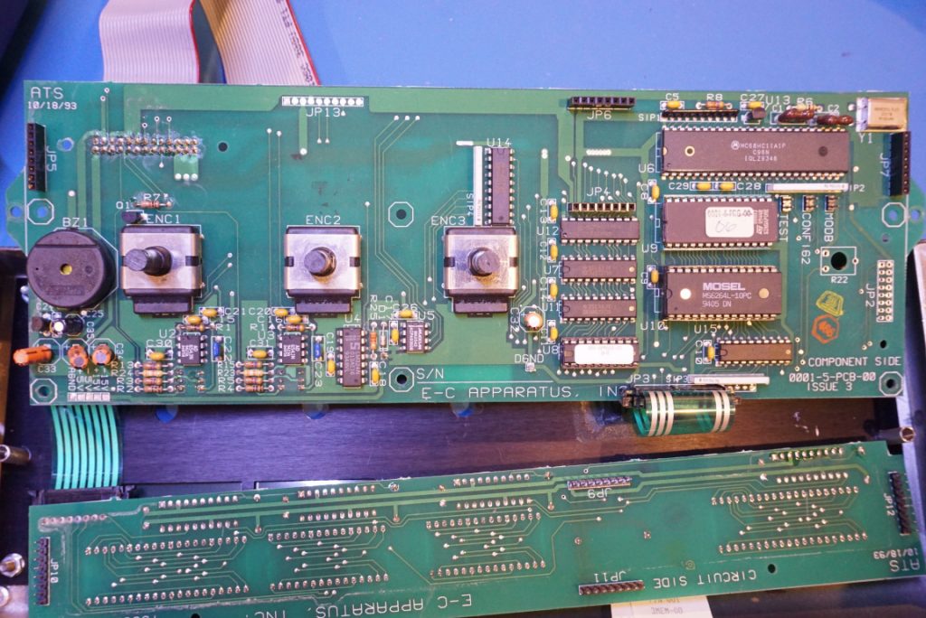
Now it’s time to take a look inside. The top cover is secured with four screws. Here is a picture showing the interior with the top cover removed. I really liked the design as the front panel is connected to the main board via a ribbon cable and it can be removed easily for servicing either half of the boards.
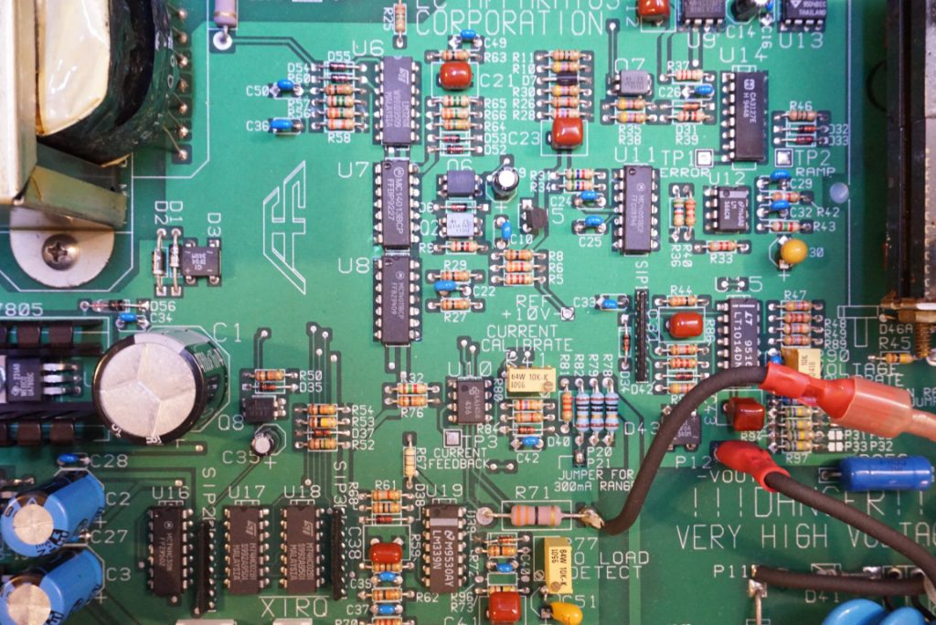
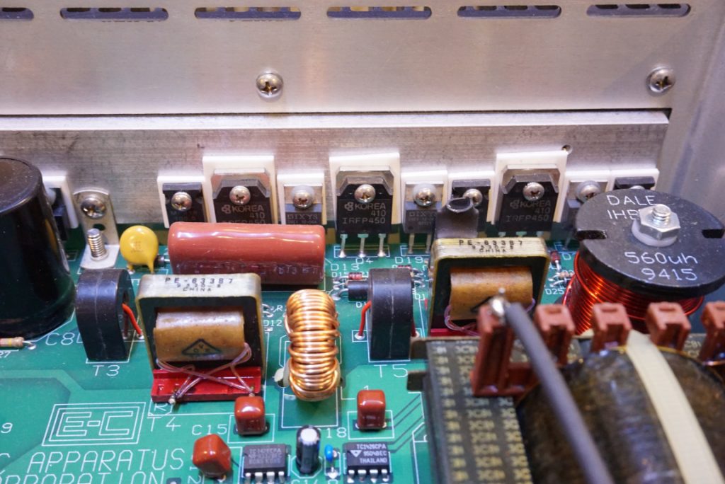
Here is a picture of the main board. While the exact topology of the power supply is not entirely clear we can infer from the TRIAC driver MOC3063 and the Thyristor 2N6344A mounted on the rear heatsink that this high voltage power supply utilizes TRIAC switching to achieve the variable output voltage.
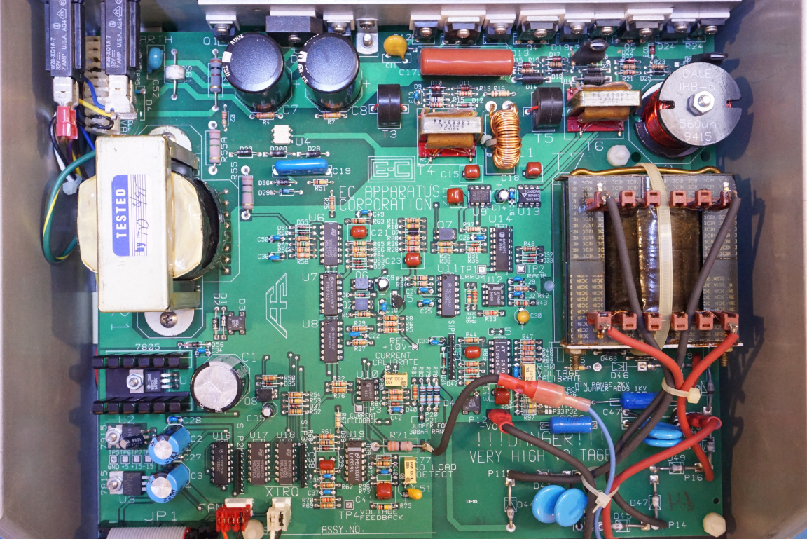
The MOSFETs used for driving the final inverter stage are IRFP450‘s, which have a Vds of 500V. The MOSFET drivers used here are TC1426CPA. There is also an LT1014DN quad precision op-amp, presumably used in the feedback loop to control the output voltage.
There is a a LM566 voltage controlled oscillator IC on the main board. Presumably it is used to generate the required pulses for the MOSFET inverter stage.
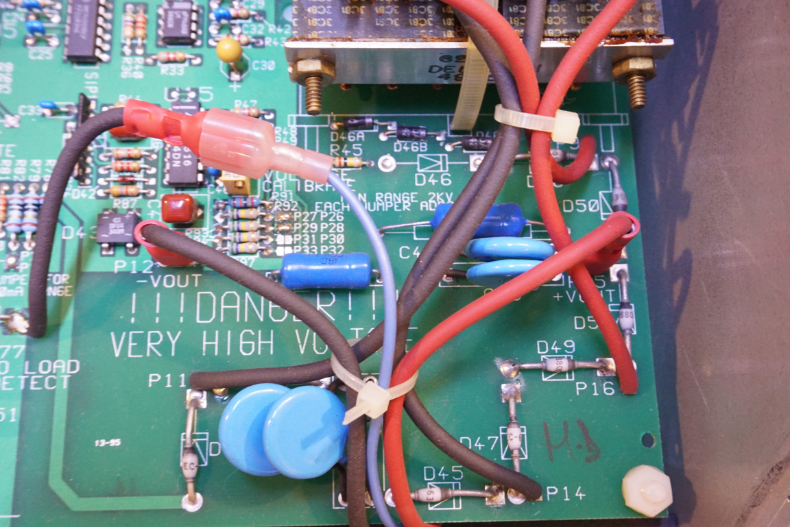
Here is a closeup of the high voltage output portion of the board. We can see many diodes connected in series so that they can withstand the high output voltage.
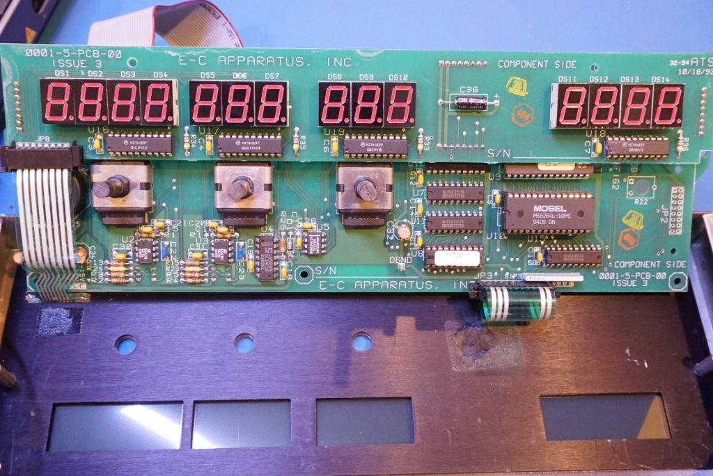
The pictures below are the front panel PCBs. There are two PCBs sandwiched together. The 7 segment display along with the MP14489 LED display drivers are on a separate PCB from the remaining front panel logic board.
The main front panel board to the right below contains a Motorola 68HC11 9bit microcontroller, along with SRAM (MS6264L-10PC) and the firmware EPROM. Three digital encoders are used for voltage/current and power limit adjustments.
Interestingly, there are a few AD654 voltage to frequency converter chips on the board. I am not entirely sure what they are used for. One possibility is that they are used as analog to digital converters. There is also a 12-bit digital to analog converter chip MAX543 in sight.
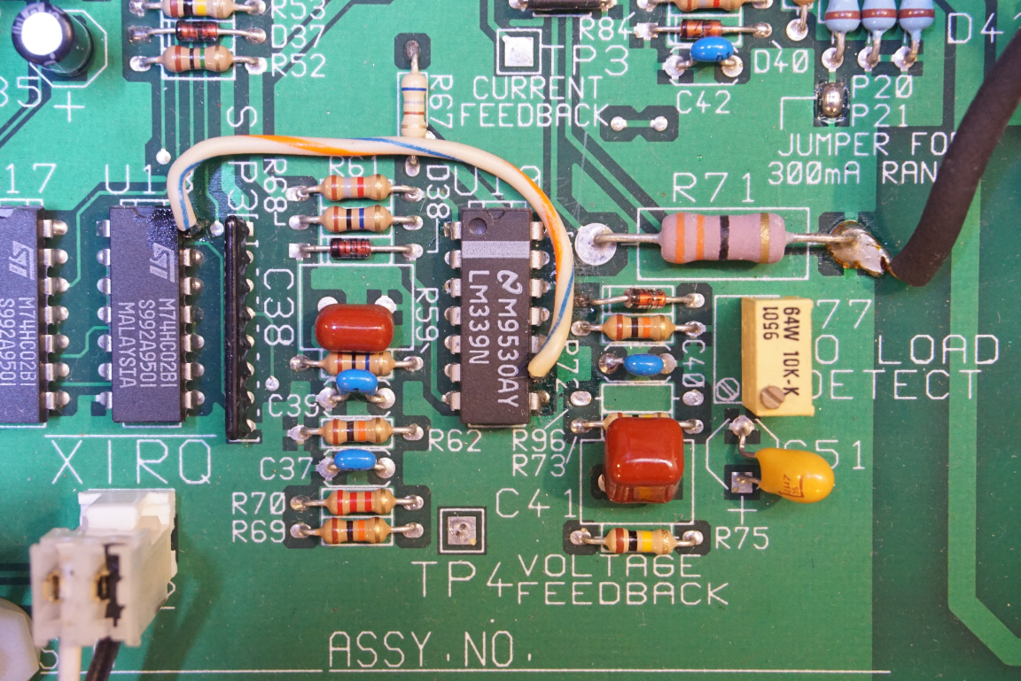
Now back to the load detection circuitry. If you look at the main board, you will see towards the bottom there is a section with the silkscreen “No Load Detect” printed. At the center of this load detection circuitry is an LM339 comparator chip.
After some testing, I figured out that comparator 3 (pin 8,9 and 14) of this LM339 is used for load detection. When load is present, the voltage drop across the sensing resistor raises the input on pin 9 above pin 8 and the output from pin 14 becomes high which in turn disables the no-load alarm. And when no load is present, the output from pin 14 is low.
To disable the no-load alarm, I simply wired the positive input to comparator 3 to an adjacent 5V rail, this overrides the sensing resistor input and worked out beautifully.
Below is a video of the this teardown.

