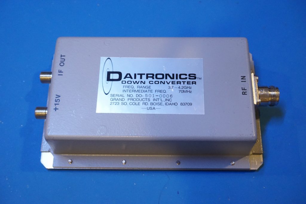
I recently picked up a downconverter box on eBay. My original plan was to use the enclosure for another project as it has a very nice aluminum enclosure. Naturally of course, I wanted to take a look at what kind of downconverter this one is and how it works first.
A down converter at its core is really just a frequency mixer. This one though is an active mixer so instead of incurring a conversion loss, it has a conversion gain at the IF output.
This Daitronics down converter has an input frequency range of between 3.7 and 4.2 GHz and operates at an IF of 70 MHz. That’s all the information there is on the label and besides that there is very little information available on the internet. At this frequency range however, it is likely that this donconverter was designed for some sort of satellite communication applications.
Upon revealing the internals, it became apparent that this downconverter is an I/Q quadrature mixer. Compared to a traditional heterodyne mixer, it does not need a bandpass filter and can be easily made tunable. For more detailed explanations, I would recommend reading this article — The Why and When of IQ Mixers for Beginners — on Marki Microwave‘s site.
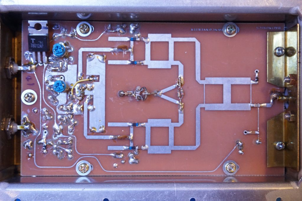
Looking at the PCB traces above, you can clearly see the two distinct two signal paths used in this quadrature mixer. The signal enters from the N connector from the right side of the PCB in the picture above. And it passes through a modified Wikinson power divider before entering the mixing stage. This modified power divider uses an “H” shaped structure, causing the signal to the upper branch to have a 90 degree phase shift.
Each branch of the signal is then mixed with the LO using a branchline coupler mixer structure, which isolates the LO from the RF input.
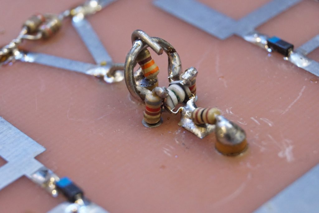
The LO signal penetrates the PCB and enters from the middle. Take a look at how this is implemented in the picture below, it is more of an art than just plain circuitry.
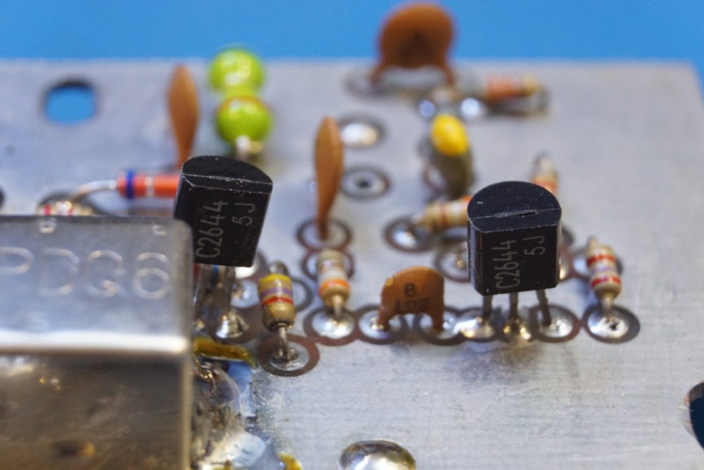
It is interesting to see a mix of bag of surface mounted components and through-hole components used in the microwave frequency portion of the circuitry.
Given the components chosen, it is clear that this design must have been several decades old. Since there is no date codes on any of the components I could find on the PCB, it is hard to tell when exactly this board was made. But from the components, the manually drawn traces and the tinned PCB, I could only presume that it was perhaps made in the late 70’s or early 80’s?
Here is a picture of the reverse side of the PCB. The circuitry on this side is responsible for generating the LO signal for mixing and amplify the IF once the RF has been mixed.
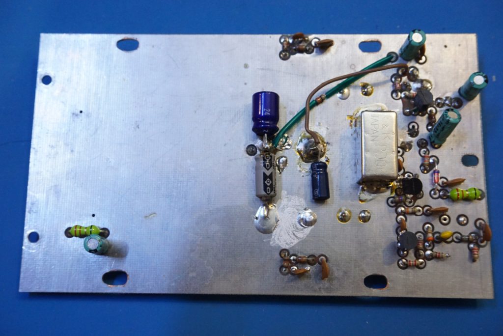
As you may have noted, none of the signal traces has ground via-stitching to help signal isolation and reducing impedance. Back in the days, PCB manufacturing was not as advanced. So instead a large continuous ground plane was used.
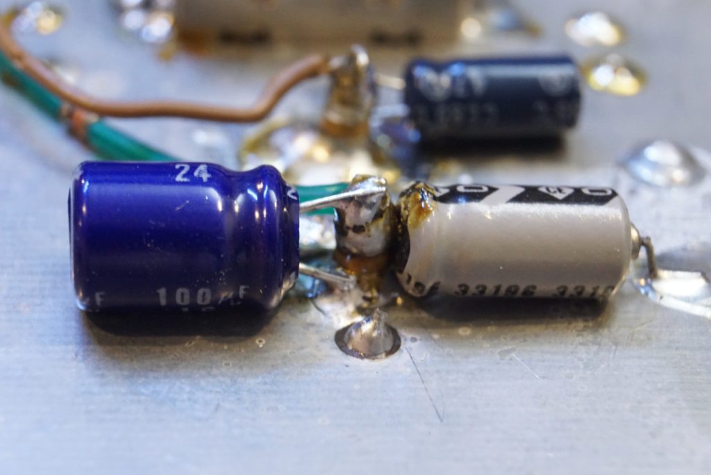
Take a look below at how filtering caps and other components are soldered. To reduce lead inductance, all connections are made as short as possible.
I also made a short video taking a look at this down converter in action and followed with a teardown. In the video, I took a 3.726 GHz signal from my HP 8671A and fed into the mixer and observed the IF signal on an oscilloscope.

