The latest addition to my lab equipment is a Keithley 230 programmable voltage source which can output up to ±100V. Unlike many of the power supplies and voltage sources I have, the Keithley 230 is capable of operating in all four quadrants, meaning it can both source and sink current in either of the output polarities. Although the current capability is limited to ±100mA.
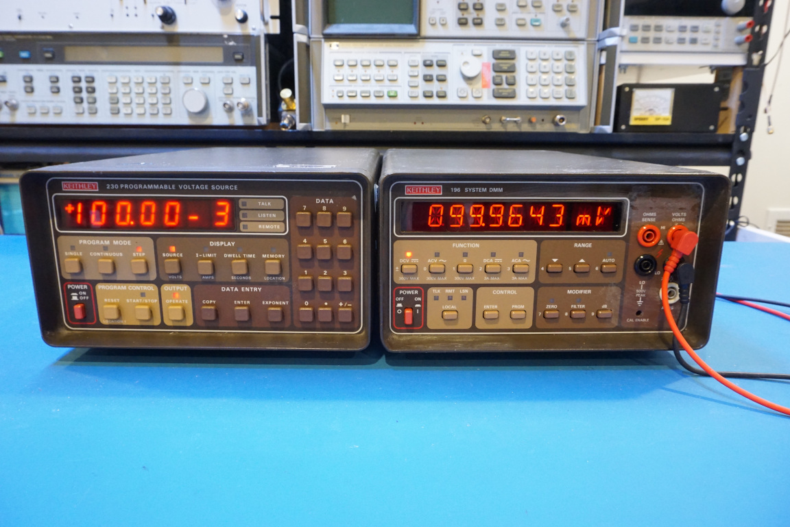
In most of its output ranges, the voltage accuracy is rated at 0.05% with a temperature coefficient of 0.005% which is quite impressive for a device in this class. The minimum voltage steps are determined by the range of operation and the resolution of the 12-bit DAC used.
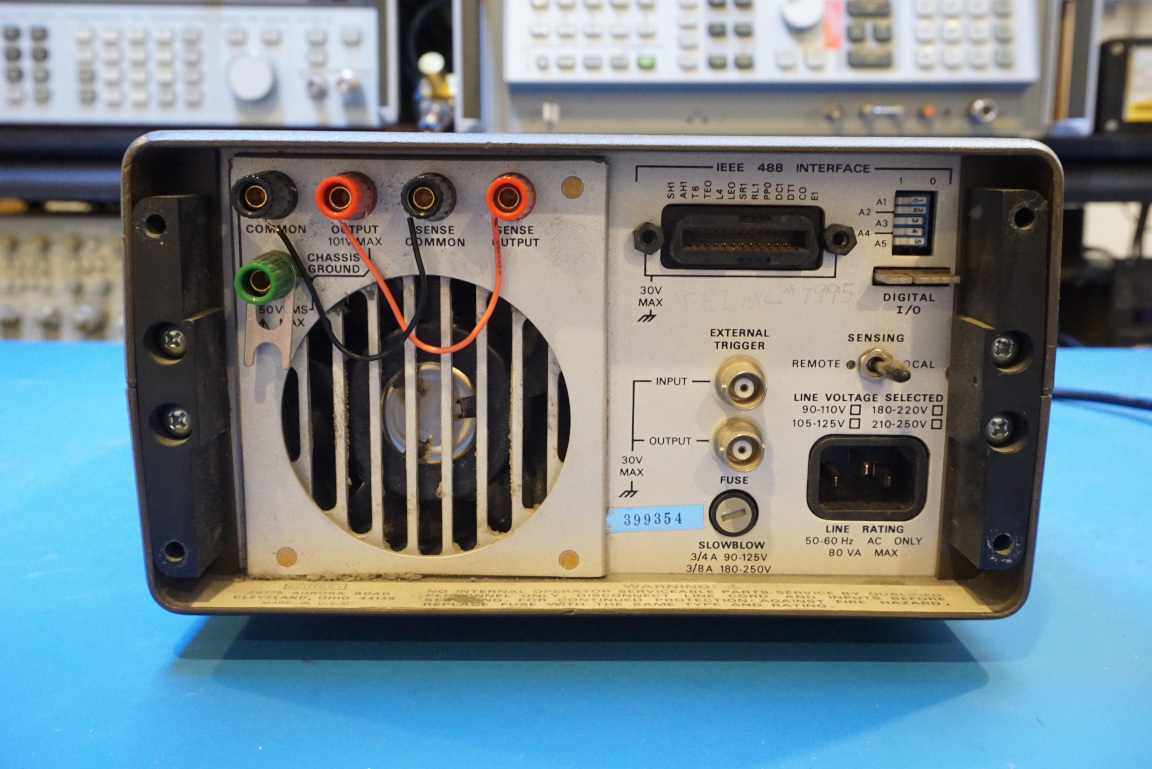
Voltage sources like this one are commonly used in automated testing environments. As you can see on the rear panel, the 230 has trigger input/output BNC connectors and digital I/O connections. Along with the GPIB connection, operator can program the 230 to perform sequences of tasks automatically.
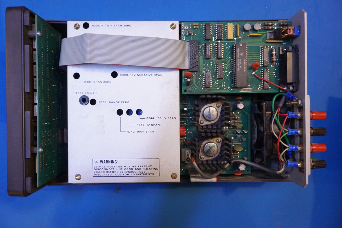
Upon removing the cover, you can see the typical clean Keithley layout inside. From the date code printed on many components, I suspect that this unit was built sometime in late 1987 or early 1988.
While I was doing some testing on the outputs from different ranges using my Keithley 196, which is a 6½ digit bench multimeter, I noticed that some of the ranges were slightly out of calibration. But considering the 30+ years of service life of this unit, it remains quite impressive that the calibration only drifted ever so slightly. And each of the adjustment points is clearly marked, making re-calibration an easy task with the right equipment.
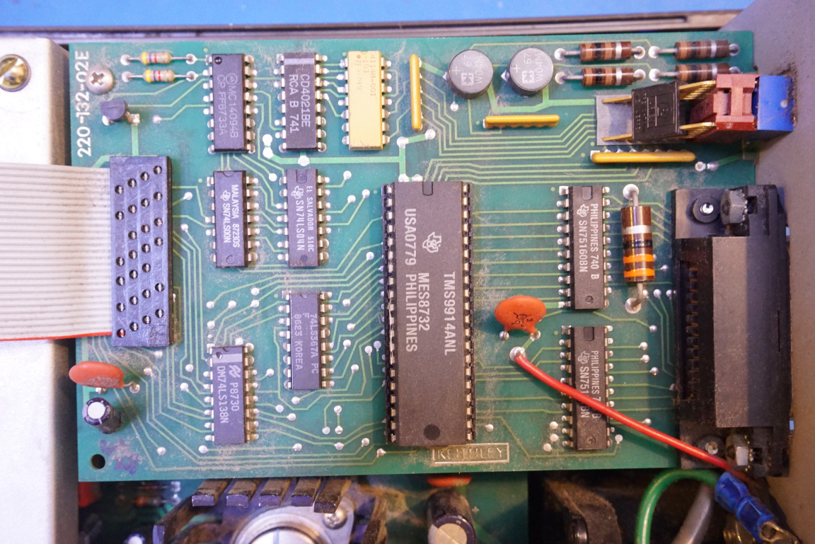
Towards the upper right corner is the GPIB/digital IO daughter board. An enlarged picture of the board is shown below.
The GPIB controller chip used here is a TMS9114A.
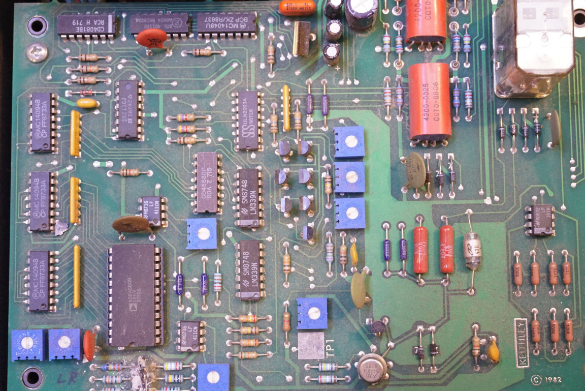
Underneath the metal shielding cover is the sensitive portion of the circuitry which is responsible for generating and amplifying the voltage output by the DAC to obtain the correct output voltage.
The two large transistors seen below (MJ15011, MJ15012) are for the final output stage after the the bootstrapped op amp circuitry to drive the output between the ±100V range.
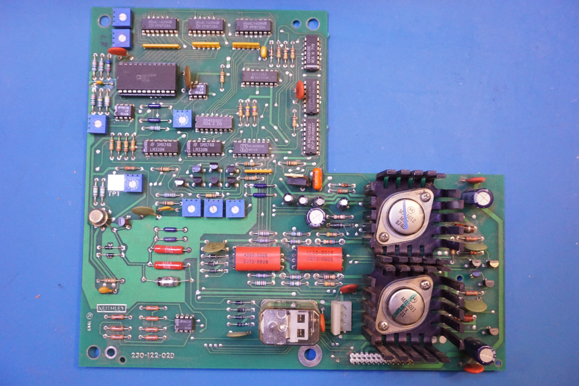
The picture below shows the closeup of what is underneath the shielding cover. At the heart of the Keithley 230 is an Analog ADDAC80N 12-bit digital to analog converter. The temperature coefficient (tempco) of the voltage reference internal to the ADDAC80N largely determines the overall temperature stability of the voltage source.
Note the damaged component towards the bottom left of the picture below. It is a 100 nF bypass capacitor for the DAC on the +15V rail. It did not cause any noticeable issue during my testing and after I dissembled the boards I replaced it with a new one (see in picture above).
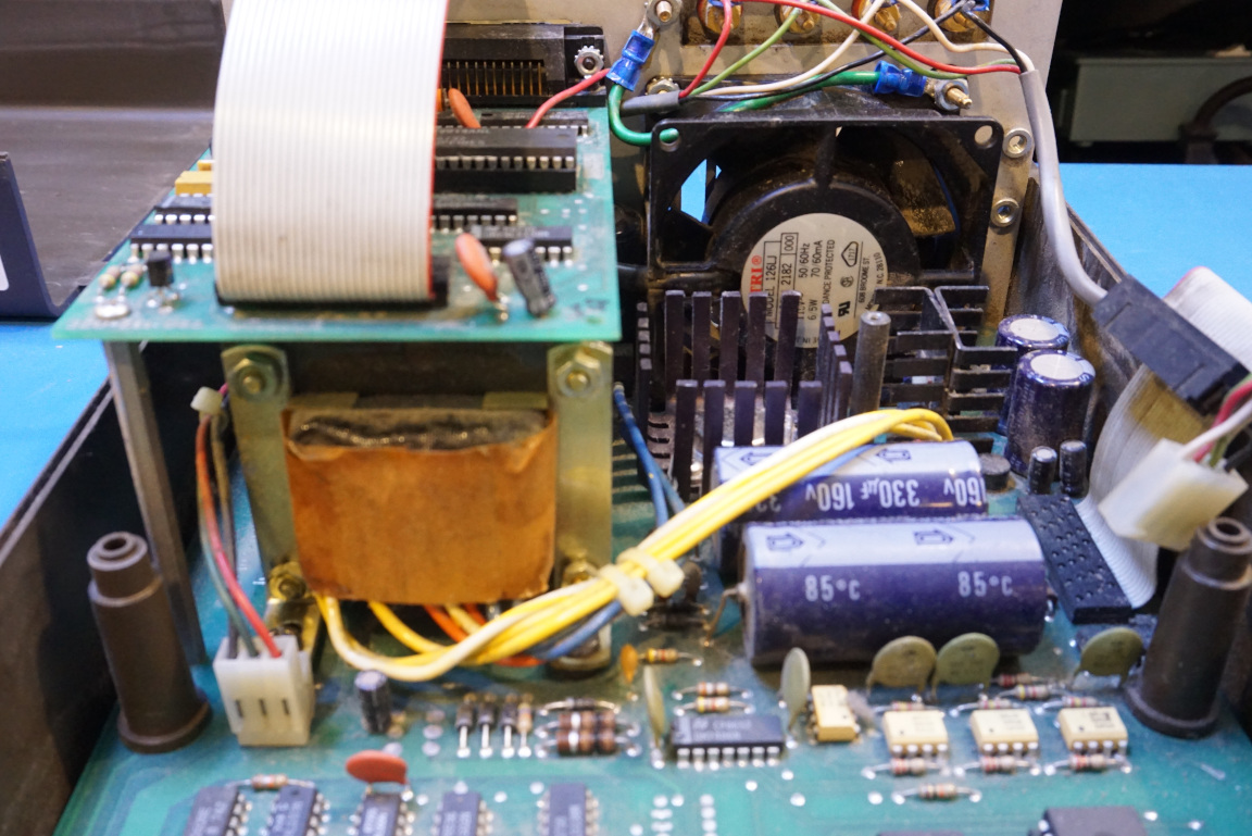
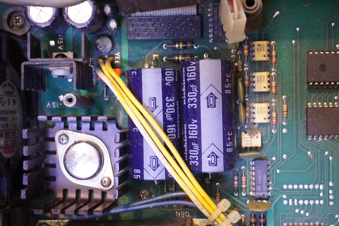
The remaining board located at the bottom of the case contains the power supply and the digital portions of the circuitry. In the picture below, you can also see the vertically mounted 7-segment display board.
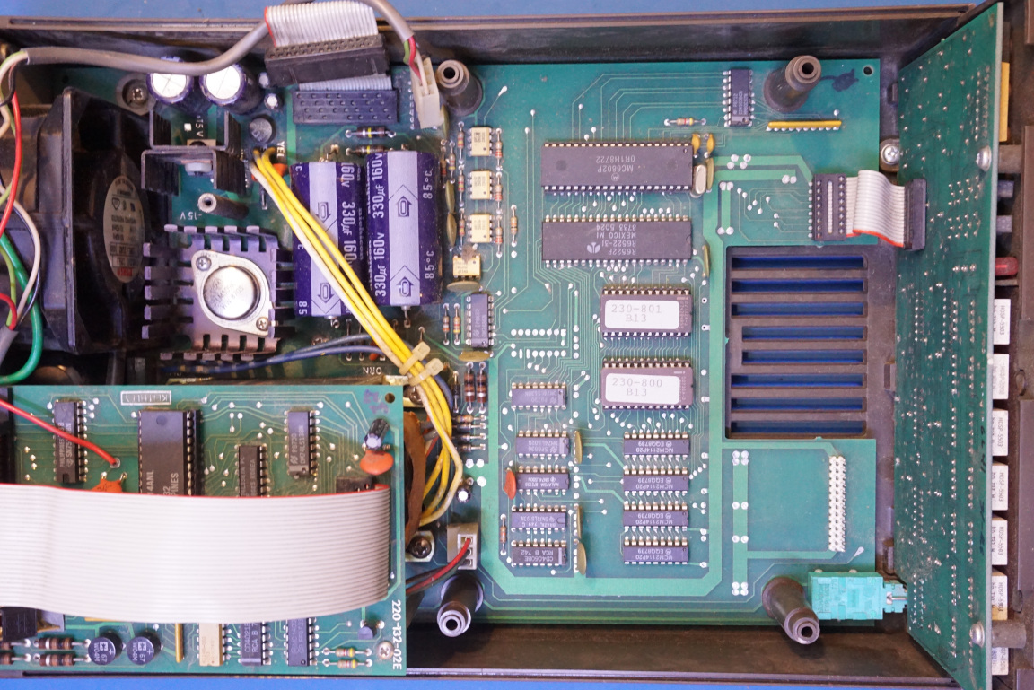
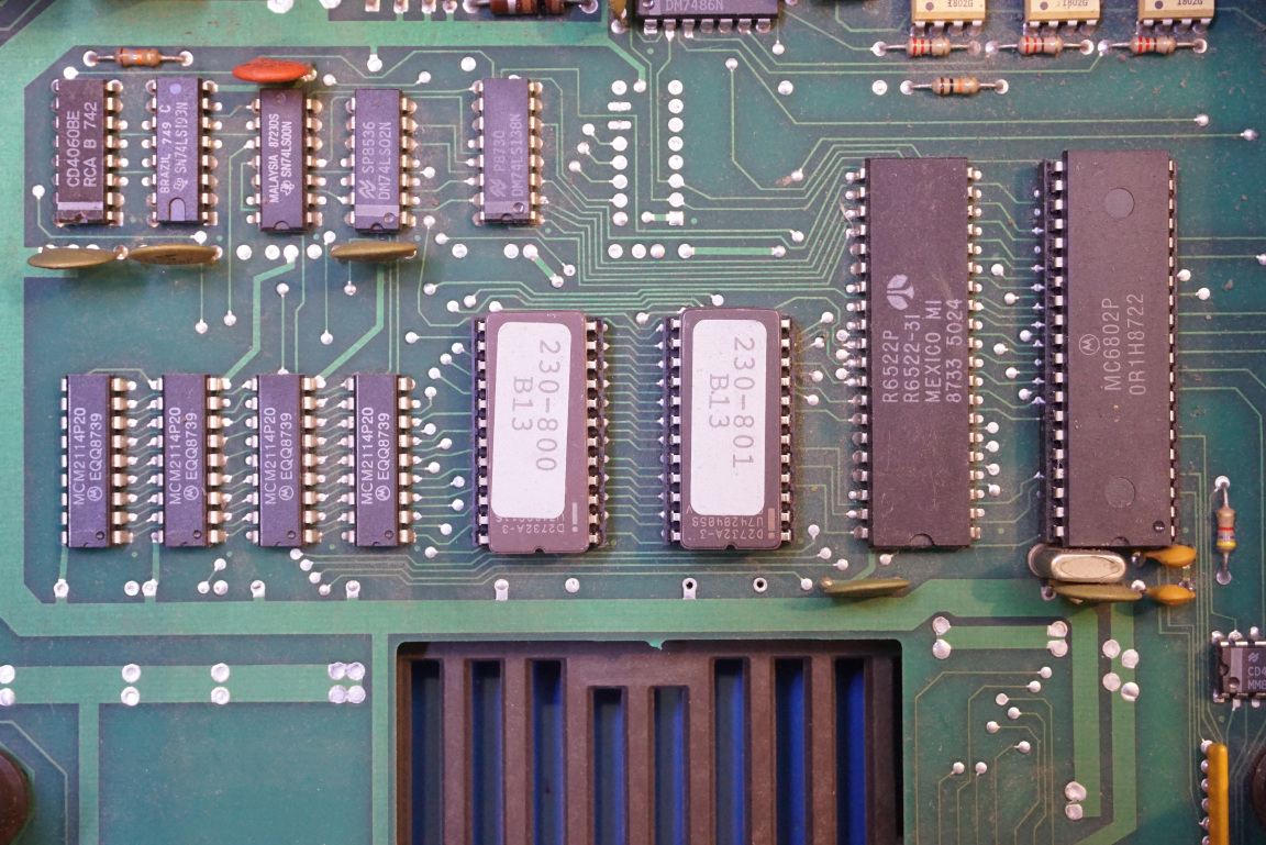
And here is a closeup of the microprocessor portion. The microprocessor used is a classic Motorola 6800 chip MC6802P. I have dumped the firmware binaries (version B13) and they can be downloaded towards the end of this post.
Here are a couple of pictures showing the linear regulator on the bottom board next to the power transformer. Note the optoisolators in the picture. These are used to isolate the control signals.
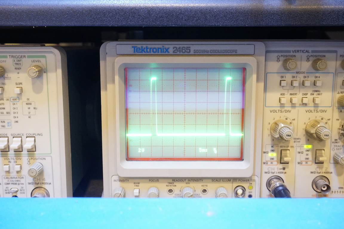
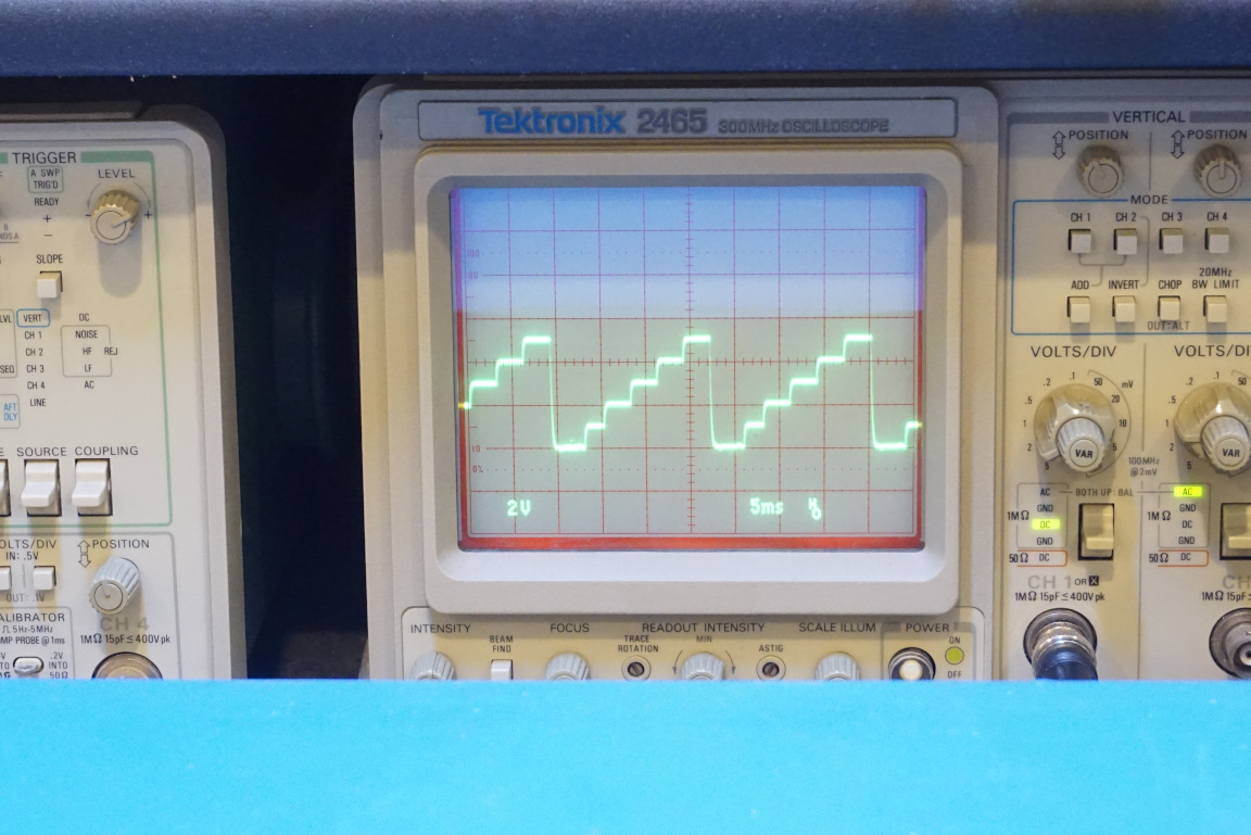
The Keithley 230 programmable voltage source has 100 onboard memory locations and each location can be programmed independently to store unique values of voltage/current and duration. With this capability, we can generate very precise arbitrary waveforms at low repetition rate.
The pictures below illustrate using the Keithley 230 to generate a pulse train and a staircase signal respectively.
A video of the teardown and experiments can be found below:

