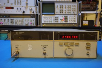
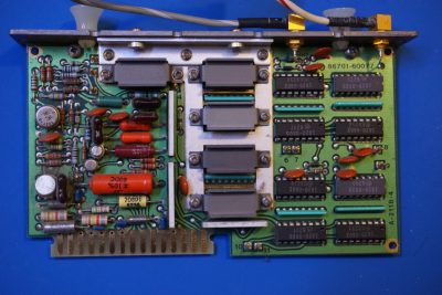
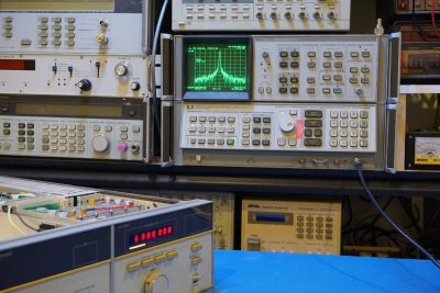
I recently bought an HP 8671A microwave frequency synthesizer on eBay. This synthesizer can generate signals from 2GHz to 6.2GHz with an unleveled output of more than 8dBm. It is a nice complement to my HP 8642B signal generator and Wavetek 907 signal generator. Using these generators, I can now generate signals of pretty much any frequencies under the 12GHz range. A video of this teardown is linked towards the end of this post.
The HP 8671A I got was an early 1980’s model. In the same series, there are also HP 8671B and HP 8672A. Both of which cover a wider frequency range up to 18.6 GHz and have leveled output. The basic operating principles however should be very similar for all these three synthesizers except for the output sections as all three use the same 2 to 6.2 GHz YIG tuned oscillators (YTO) and the extra frequency range in the other two models are achieved via YIG tuned frequency multipliers.
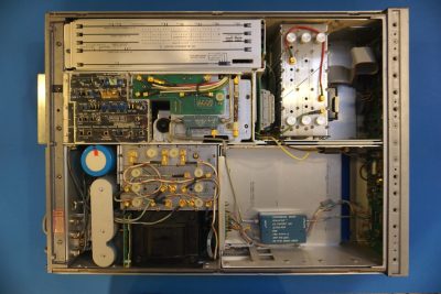
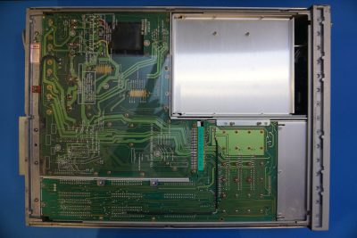
Like many Hewlett Packard test equipment back in the same era, the top and bottom panels are each secured via a single captive retaining screw and the panels slid off easily after the screws are loosened.
|
|
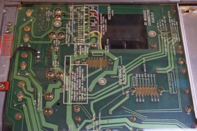
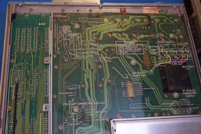
As you can see from these pictures, this unit was clearly designed with serviceability in mind as most of the test points are clearly marked and accessible with the removal of either the top or the bottom panel (click on picture to see the full sized version of the image).
|
|
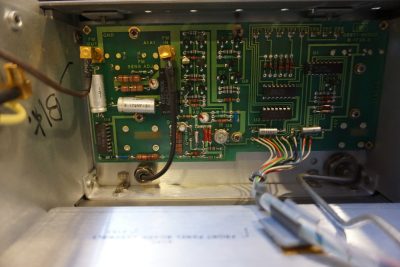
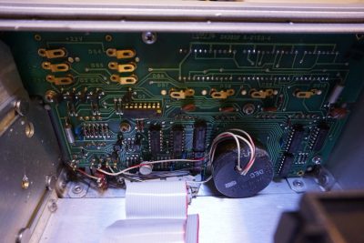
The front panel circuit board houses the digital display portion and the rotary encoder input along with other range setting switches. Again, test points and voltage references are clearly marked for easy troubleshooting. From the style of the instrument panel light clips, we can infer that those are probably incandescent bulbs rather than LED ones. From the datecode (1982) on the rotary encoder and other components we can infer an early 1980’s manufacturing date.
|
|
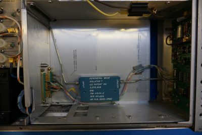
The output section of the HP 8671A is surprisingly barren. There is only a single isolator connected via rigid coax located in that section. This is because that 8671A offers only the base frequency range up to 6.2GHz and does not have any output frequency multiplication/attenuation or amplitude leveling circuitry. For 8671B and 8672A, this section is fully occupied.
The components placement inside the HP 8671A are grouped into several sections of logical groups. And daughter boards are used in each group to plug into the main board at the bottom of the chassis via board-to-board edge connectors.
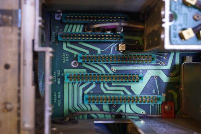
First, let us take a look at the digital section located under the aluminum plate as seen in the picture to the left below. And the picture to the right below shows the edge connectors after all the daughter boards in the digital section had been removed.
If you look closely you can just make out the ovenized crystal oscillator tucked under the YIG oscillator board in the middle section.
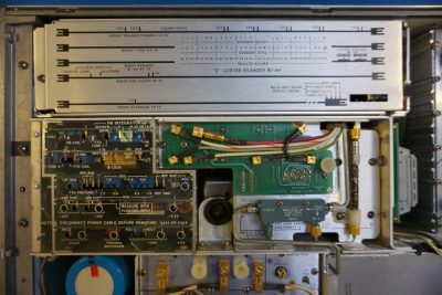
|
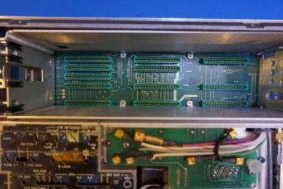
|
Plugin boards are removed one by one from the bottom to top. The first one is the A2A7 interface assembly. The four LED indicators on top indicate whether each PLL (YTO loop, Fractional N PLL, etc.) is locked.
[adsense]
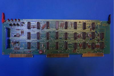
Next is the A2A8 output register assembly. From the closeup picture to the right, you can see a few components that are professionally bodged together. The way these components are mounted is likely due to PCB routing limitations rather than being an afterthought. I am not sure though why only the multiplexer register 74LS298 is socketed.
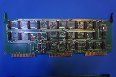
|
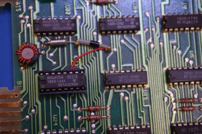
|
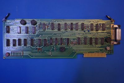
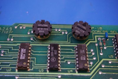
The next one is the GPIB board. In the picture to the right you can see the switches used to set the GPIB address. The entire functionality provided by this board was easily replaced by single VLSI GPIB chip in newer equipment nowadays.
|
|
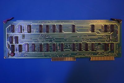
Now moving onto the A2A10 register assembly.
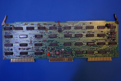
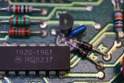
Here are a couple of pictures of the A2A11 timing and control board. Again, there is another “bodge” in the closeup picture on the right.
|
|
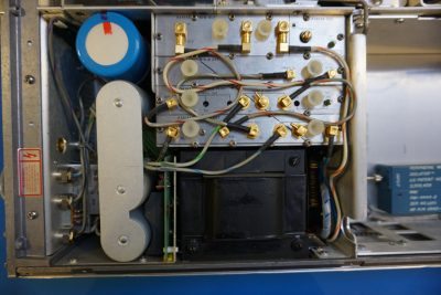
The second set of daughter boards are located in the compartment with the plexiglass cover. Here is a picture showing the connectors after the plugin boards had been removed.
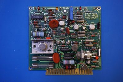
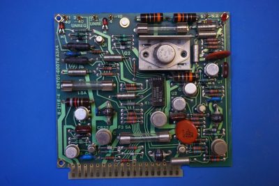
The first two boards are the positive and negative regulator boards. The power transistors seem to have been bolted onto the heatsinks.
|
|
The positive regulator board employees a crowbar overvoltage projection circuit. Here is a picture of a closeup of the SCR that serves as the crowbar in the event of an overvotlage. When an overvoltage situation occurs, the SCR is triggered and all the output current from the regulator is dumped into the SCR essentially shorting the power supply output so that other connected components are not subjected to the erroneous and potentially dangerous voltage level. The SCR is beefy enough to withstand the high current. This short current will likely blow the input fuse and shutdown the power supply entirely.
[adsense]
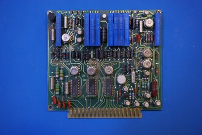
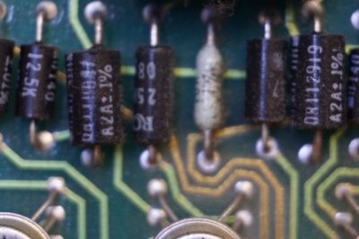
Next in the picture is the digital to analog conversion (DAC) board. The conversion accuracy is guaranteed by the precision resistors which can be seen in the picture to the right below.
|
|
Here is a picture of the YIG tuned oscillator (YTO) driver. Interestingly, the power transistor used on this board is not bolted onto the heatsink as is with the power supply board.
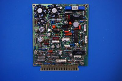
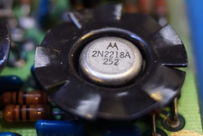
And the picture below shows the YIG FM coil driver which tunes the resonant frequency of the Yttrium iron garnet sphere. You can see heatsinks on a few of the metal can transistors, those are probably responsible for driving the coil.
|
|
Now moving onto the PLL section. The operating frequencies in this section is up to a couple of hundred MHz and thus each board is individually shielded within a metal can compartment. In the pictures below, the plugin cards were taken out from left to right.
The YIG oscillator is located on the left partially out-of-view. I did not take out the YIG oscillator as there are quite a few rigid coaxes needed to be disconnected first. If you are interested in the internals of YIG oscillators, you can take a look at my blog post on the Wavetek 907 teardown.
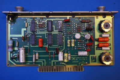
The first one is the 20/30 MHz divider board. You can see from the board layout (the continuous ground plane) that the right portion of the board probably operates at higher frequencies.
And here is a picture of the A2A4 phase detector board.
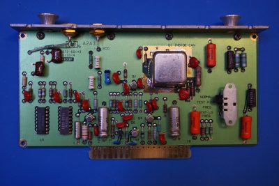
The VCO board is shown in the next picture. From the board design (almost the entire board is covered by the ground plane), we can tell that this board operates at even higher frequencies.
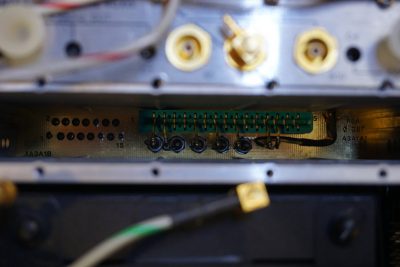
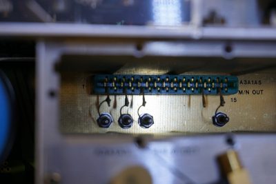
It is also interesting to see how some of the signals from the edge connectors are routed.
|
|
[adsense]
Now let’s take a look at the fractional N PLL section. The boards shown below will be from the top to the bottom.
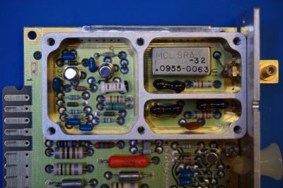
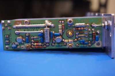
The first plugin board is the M/N PLL output and VCO board. Again the board design suggests that this circuitry operates at higher frequencies. The metal can on the left contains some filtering and other sensitive circuitry. The shielded circuitry on the right contains the VCO for the M/N PLL (I didn’t open up the VCO shielding).
Due to the high frequency, even short point to point connections are done using rigid coax.
|
|
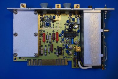
The picture below shows the M/N phase detector board. Some of the ICs on this board have heatsinks on them.
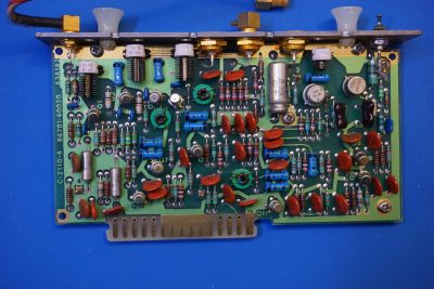
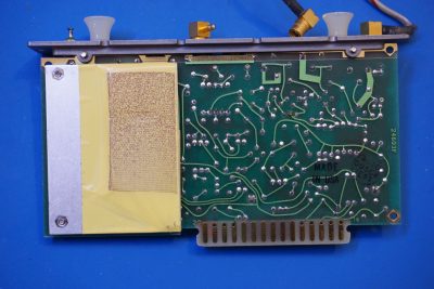
And here are a couple of pictures of the VCXO. A few air trimmer capacitors are used for fine-tuning the frequencies.
|
|
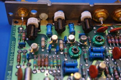
Here is a picture showing the close up of the air trimmer capacitors.
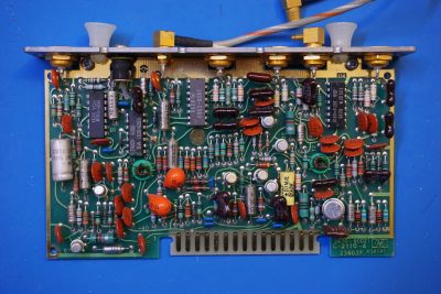
And finally here is a picture of the phase detector board for the fractional N PLL.
The picture below shows a 6GHz tone on my HP 8566B spectrum analyzer. Phase noise from the PLL can also be seen.
A video of some measurements and the teardown is included below:
