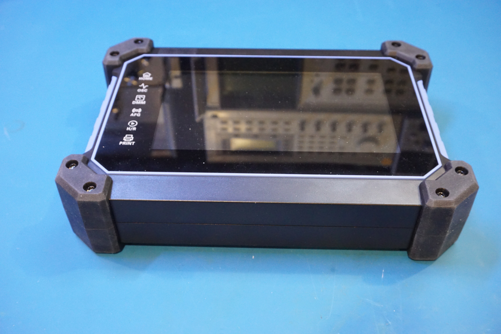
In a recent video, I reviewed a Hantek TO1204D quad channel 200 MHz digital oscilloscope/DMM/AWG combo device. In this blog post, let’s take a look at some of the teardown pictures.
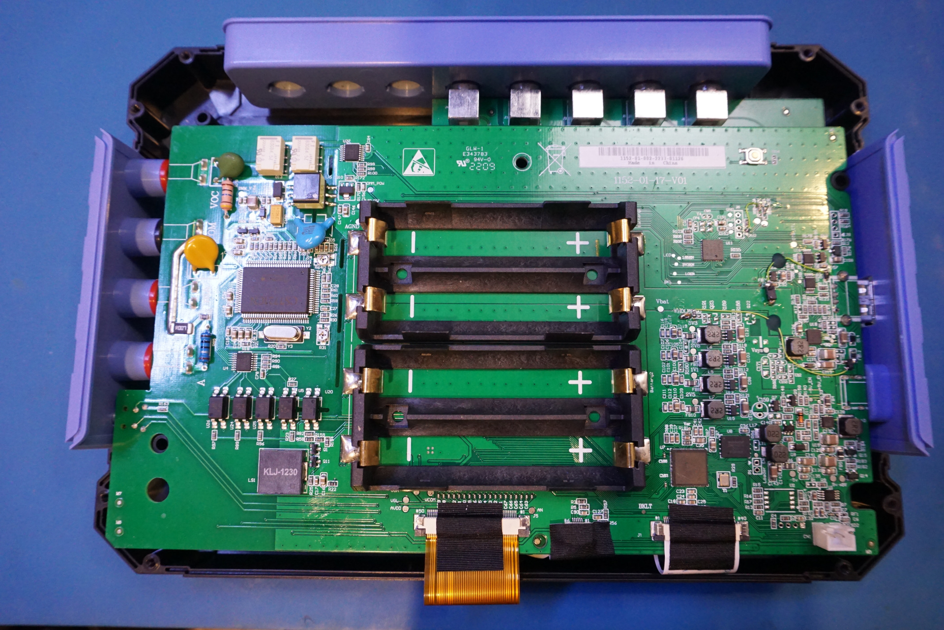
The scope uses a two board design. Upon opening the back cover, you can see the main board (left), which is stacked on top of the board dedicated for the oscilloscope and arbitrary waveform generator.
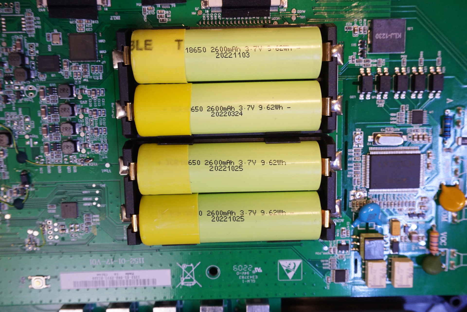
TO1204D uses four 2600 mAh 18650 cells.
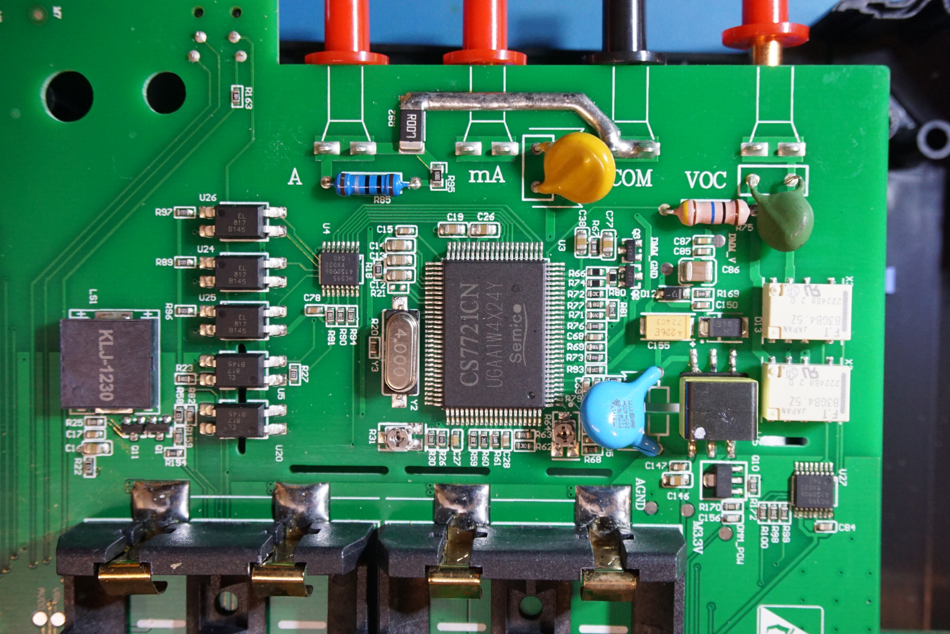
The builtin multimeter is only a 4000 counts one, which is essentially the same as what’s in the Hantek 2D72 handheld oscilloscope, which is based on a CS7721CN DMM chip. Unfortunately, the high current measurement range is not fused, it relies on a 7 milli-Ohm shunt resistor as the fusible element. Besides a PTC and a poly fuse for the mA range, there is not a lot of protection circuitry for the input section.
In the picture to the right below, you can see several bodge wires. Note that there are quite a few DC-DC converters on this side of the board, they are used to produce the multiple DC rails required by the FPGA and other chips. Also note that the markings on several chips had been removed.
The two SOICs near the USB port are RS2227 1:2 USB muliplexer switches. And the 8 pin chip next to the 2 pin speaker connector is a LM4890 audio power amplifier.
In the image to the right you can also see an MSP430FR2355 MCU.
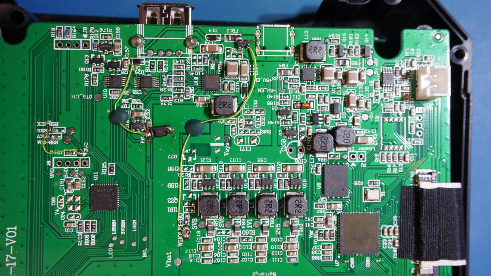
There are just a few components on the reverse side of the main PCB. You can see the current balancing circuitry at the cathode of each lithium ion batteries. They are consist of an opamp, a MOSFET and a current sensing resistor.
The picture to the right shows a close-up view of the LCD biasing circuitry. A TPS65150 is used here.
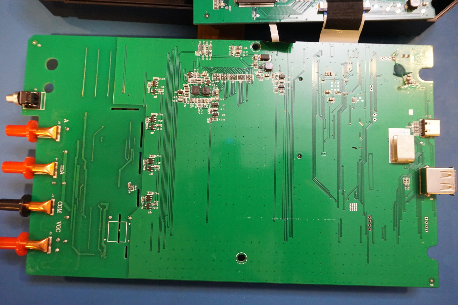
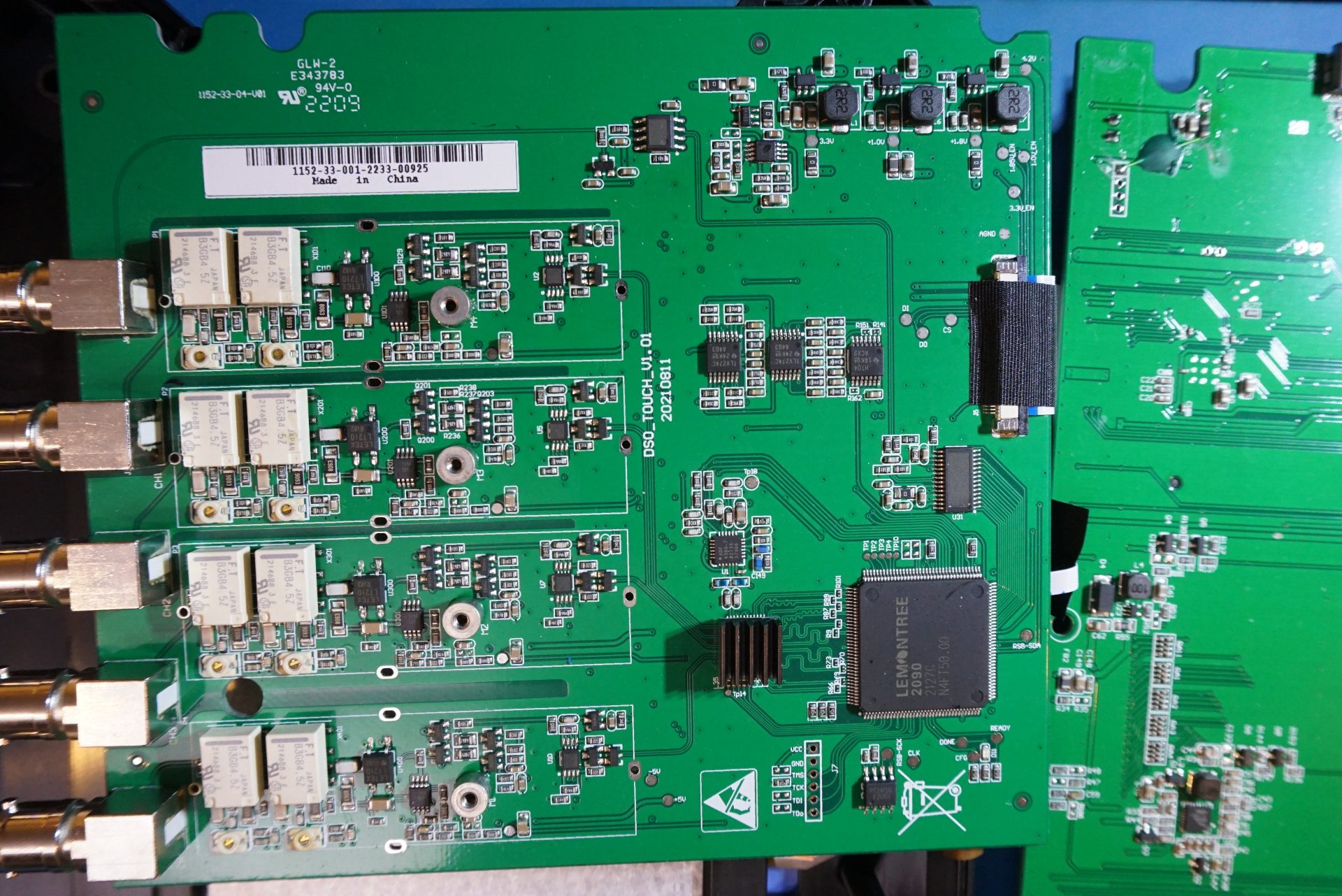
Here is a picture of the main board that’s responsible for the oscilloscope, DMM and AWG.
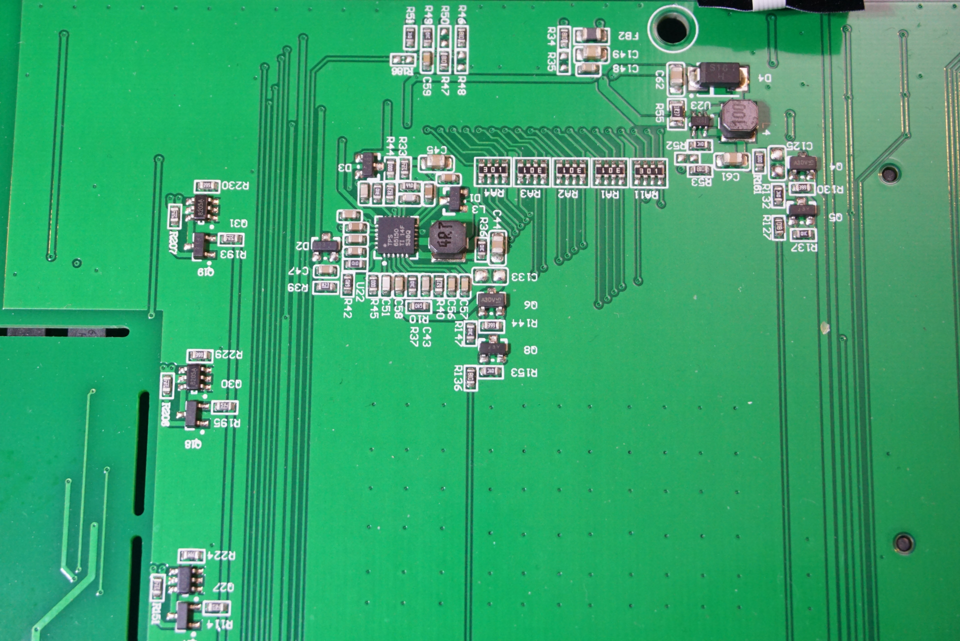
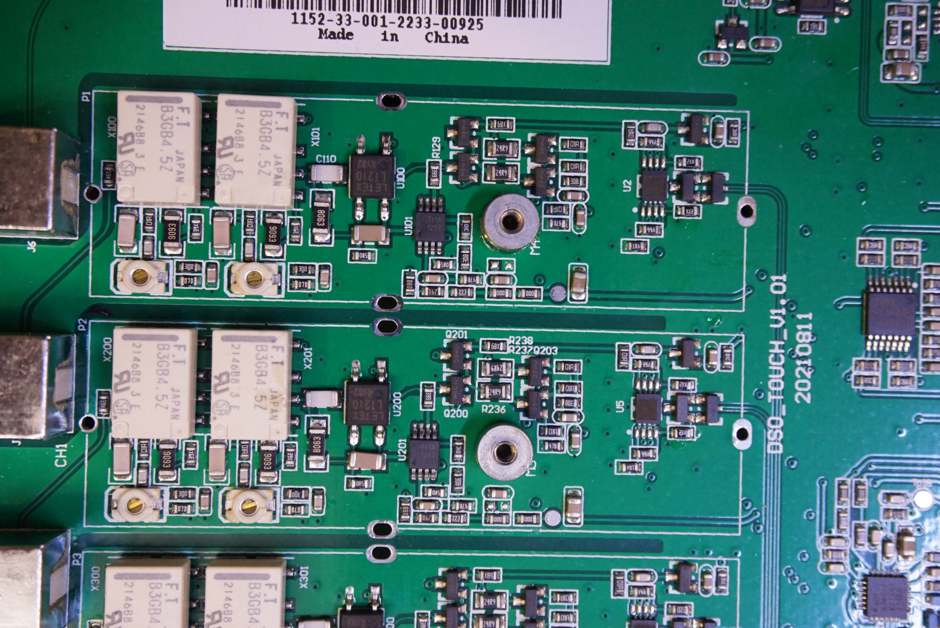
Here are a couple of pictures showing the oscilloscope input sections. The shielding cans had been removed. The input section circuitry is fairly standard, there are a couple of mechanical relays and a solid state relay for range switching. Interestingly enough the 8 pin chip towards the channel output side has its marking sanded off. It seems Hantek really went out of its way to ensure the circuit could not be easily reverse engineered.
The first BNC channel on the top corresponds to the AWG output. If you follow the trace you will see that the AWG output is driven by an OpAmp which converts the differential signal from the output DAC to a single ended signal. Unfortunately, the markings on both the DAC and OpAmp had been removed purposefully.
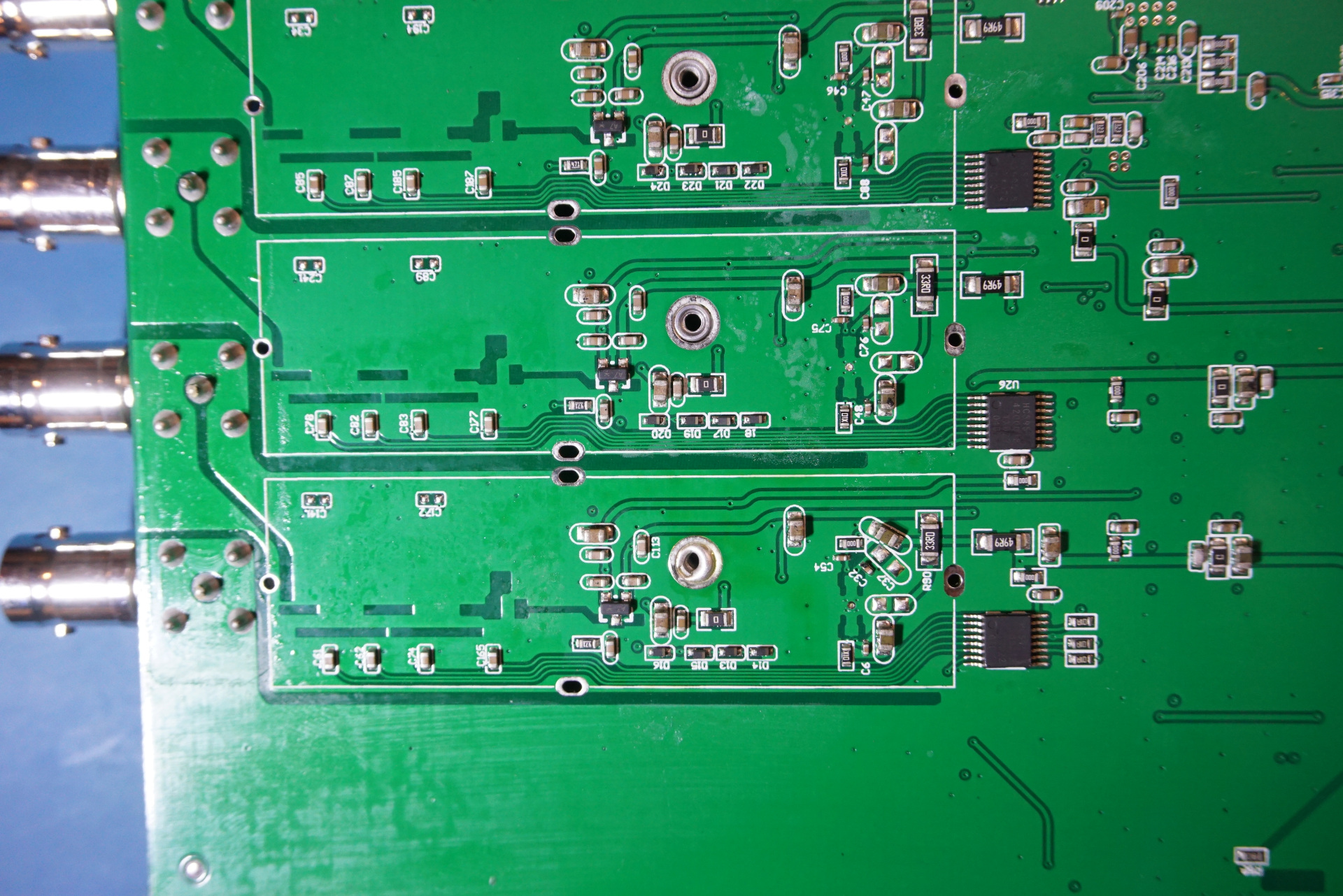
Here is a picture of the reverse side of the input section, there is a 595 shift register for each channel, perhaps they are used for setting gains and switching the relays based on the trace layout.
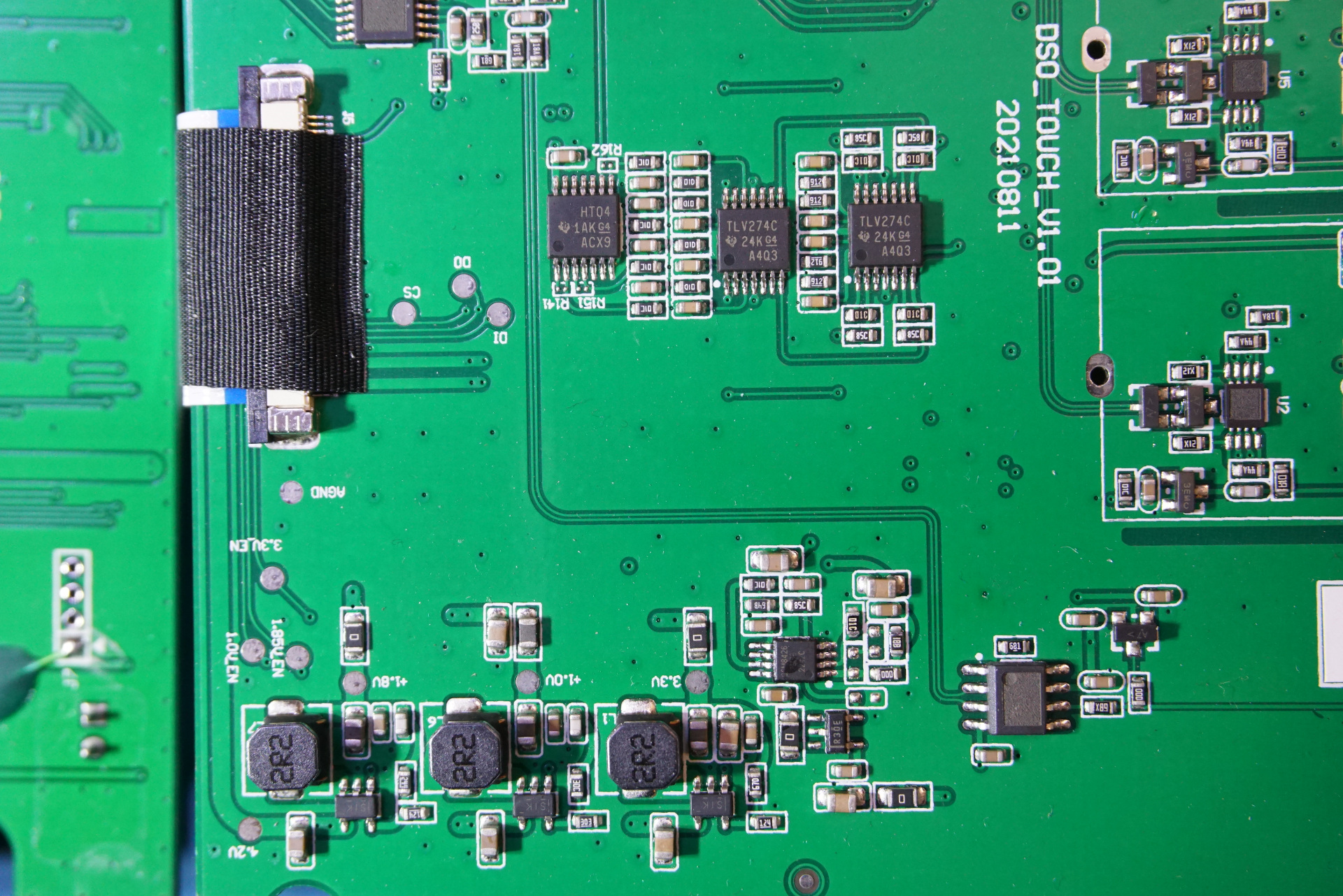
Back to the other side of the board. In the picture to the left below you can see a couple of TLV274 quad rail-to-rail Opamps. There are additional DC/DC converters on this side of the board as well.
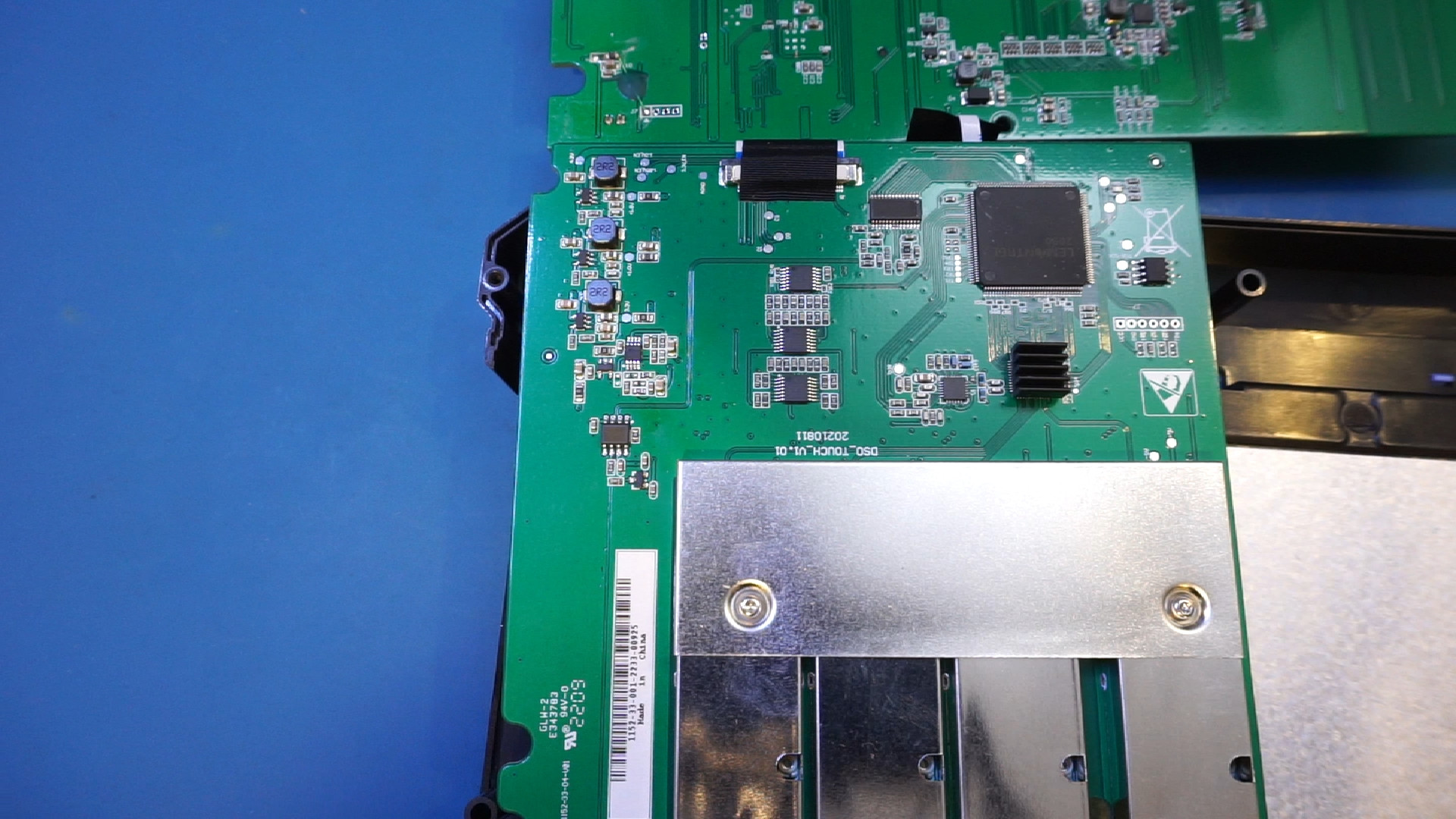
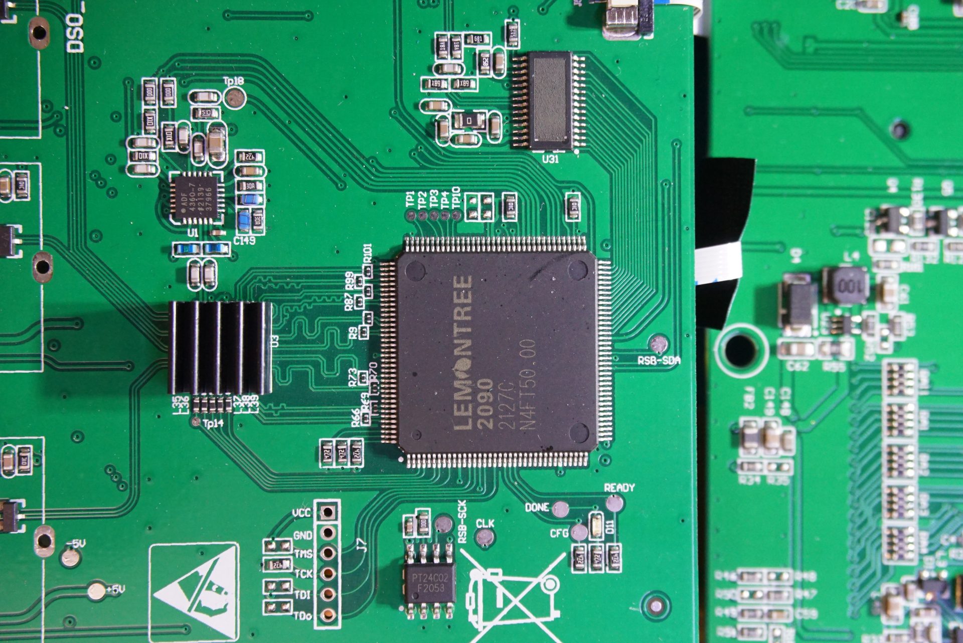
The main FPGA used is an LemonTree 2090 which is the same FPGA used in the Hantek 2D10, Unfortunately, there is not a lot of information on this chip. The chip with the heatsink must be the input ADC.
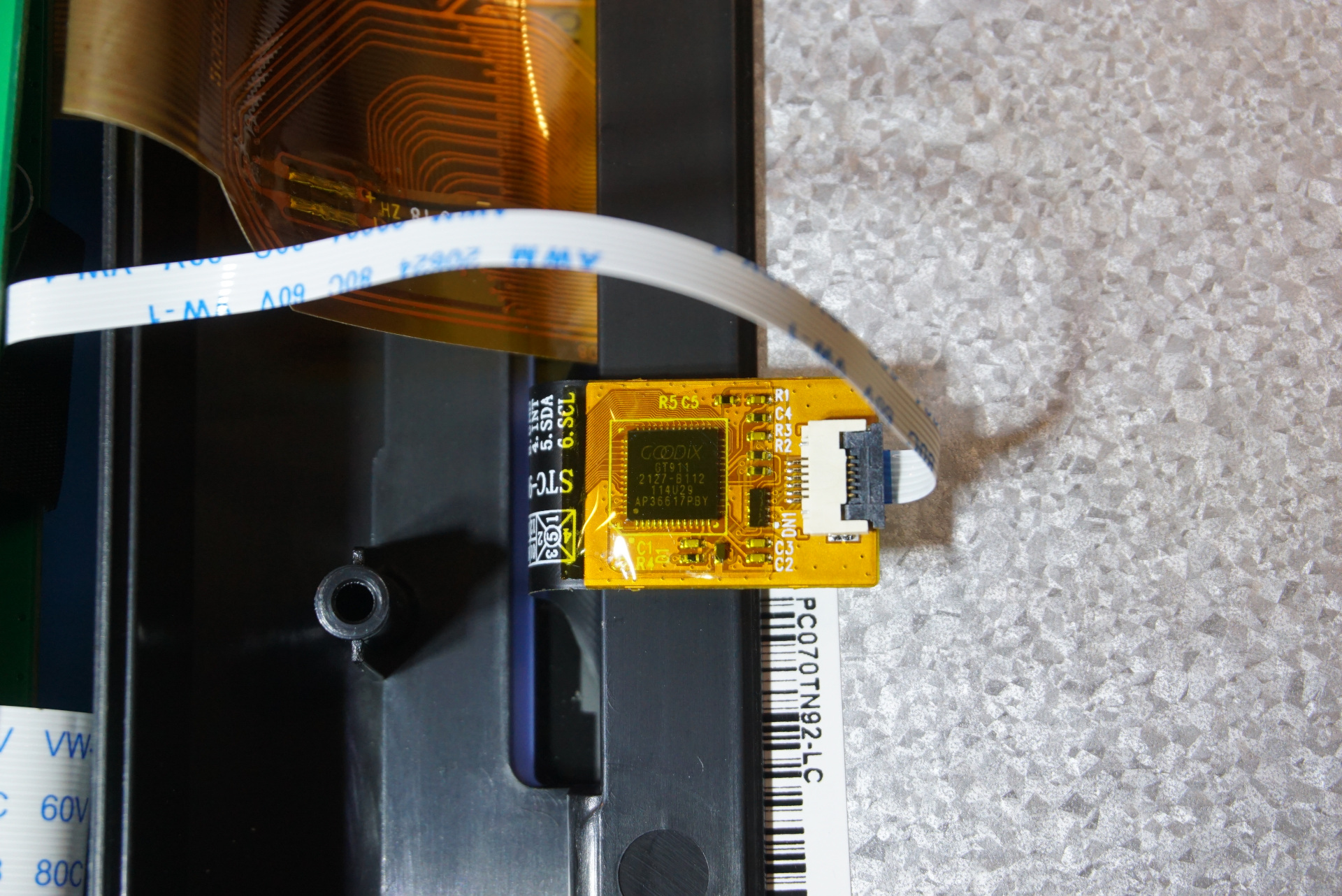
Finally, the LCD has a builtin GT911 touchscreen controller as you can see in the picture below.
You can check out the teardown video for more details:

