I did a review and teardown of DreamSourceLab’s top-of-the-line DSLogic U3Pro32 32 channel 1 GHz sampling rate logic analyzer (see video below), and in this blog post, let’s take a look at some of the teardown pictures.
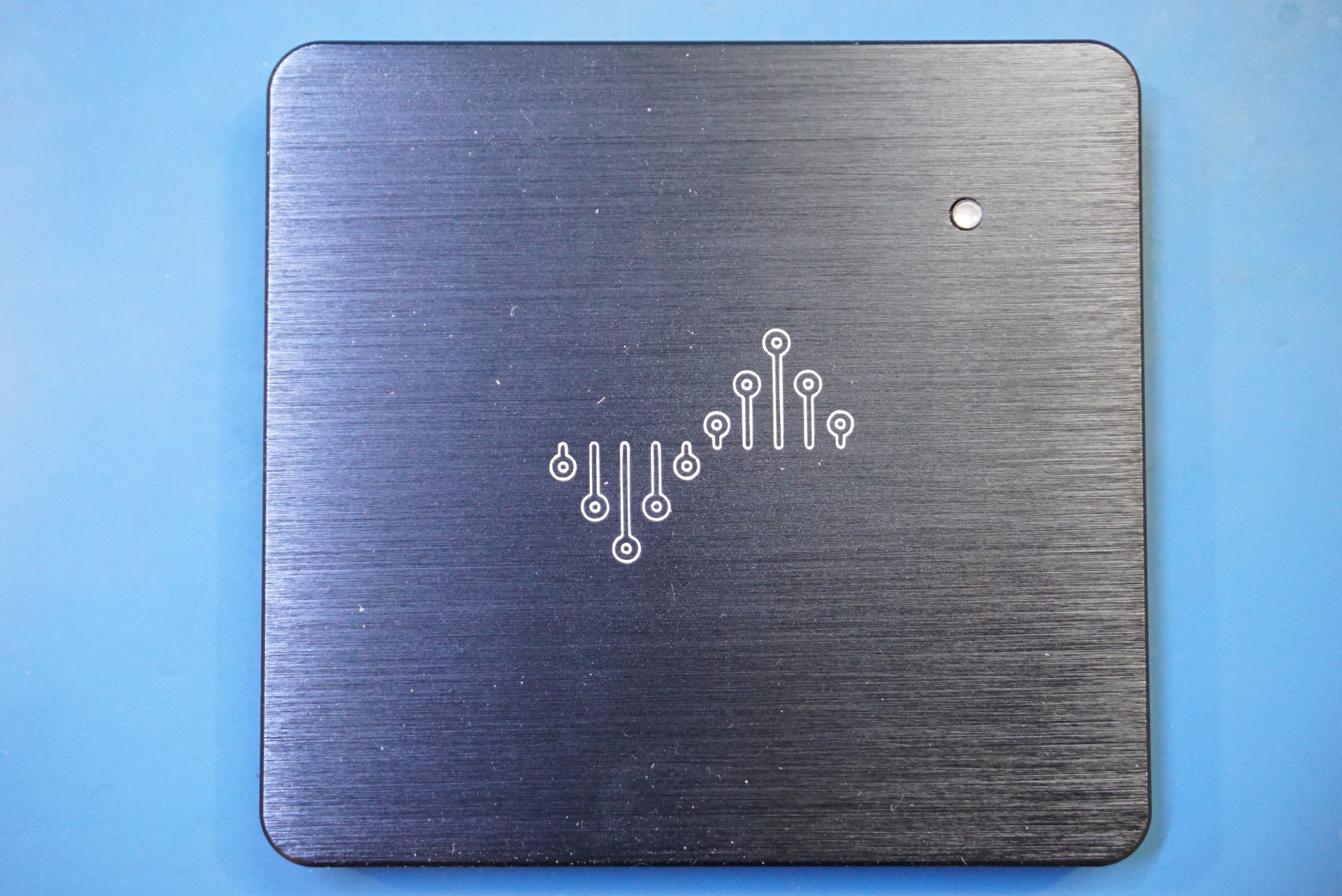
The logic analyzer is very compact, measuring just 79mm x 74mm x 9mm. It has 2 GB on-board buffer DDR memory and is capable of sampling at 1 GHz with up to eight enabled channels in buffered mode. The stream mode which captures data through the USB connection directly is limited to the maximum rate supported by the USB port on the other hand.
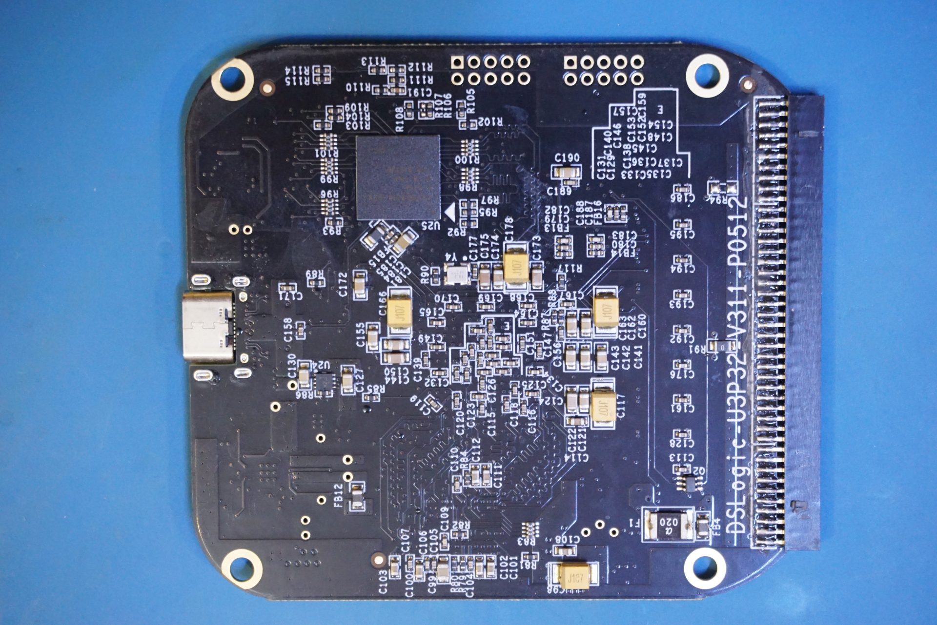
The picture below shows the reverse side of the PCB once the cover was removed. The main chip on this side is a CYUSB3014-BZXC USB controller. It is a rather capable controller and it has a 32-bit ARM926EJ core ARM processor builtin.
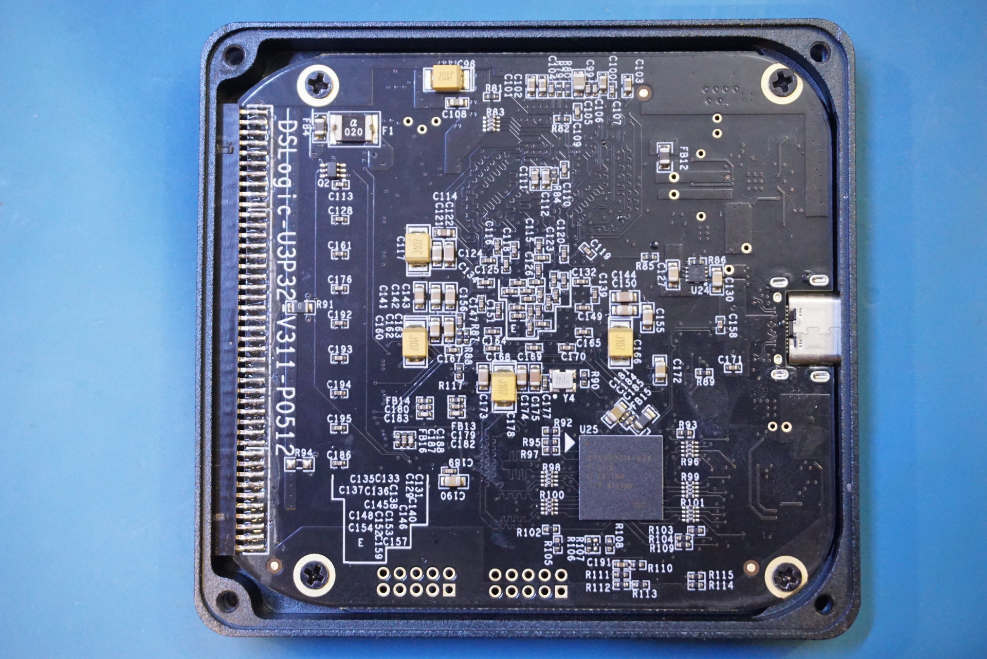
The main circuitry is on the other side of the board.
The DSLogic U3Pro32 is powered by a XLINX SPARTN 6 XC6SLX16 FTG256DIV2237 FPGA. This is essentially the same FPGA used in the DS4T1012 handheld oscilloscope. To the upper left of the FPGA, there is an ADF4360-7 integrated synthesizer and VCO. Again DS4T1012 uses the same synthesizer. Just below the FPGA in the picture to the right below, there is a 2 GB DDR3 chip which is the onboard buffer memory.
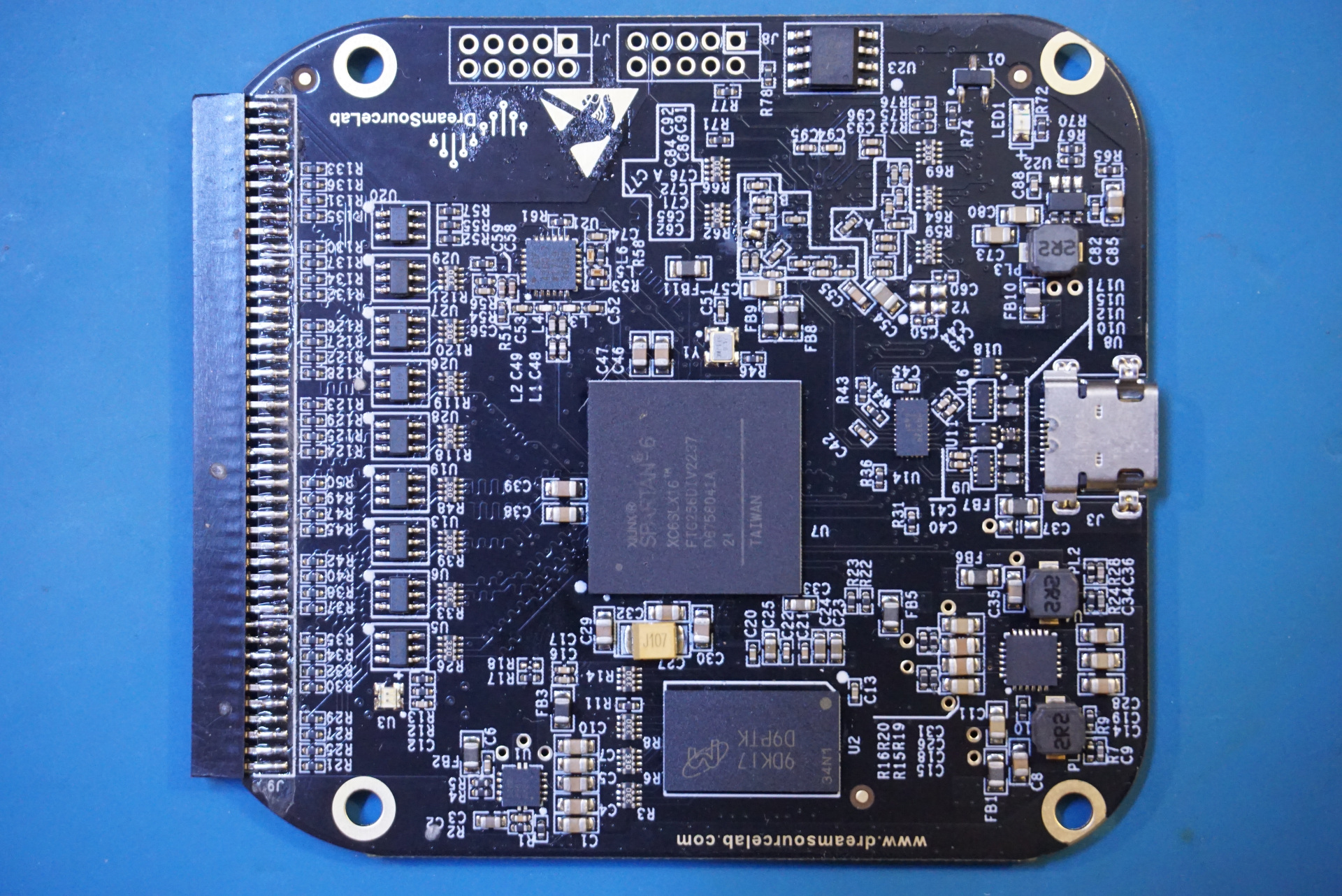
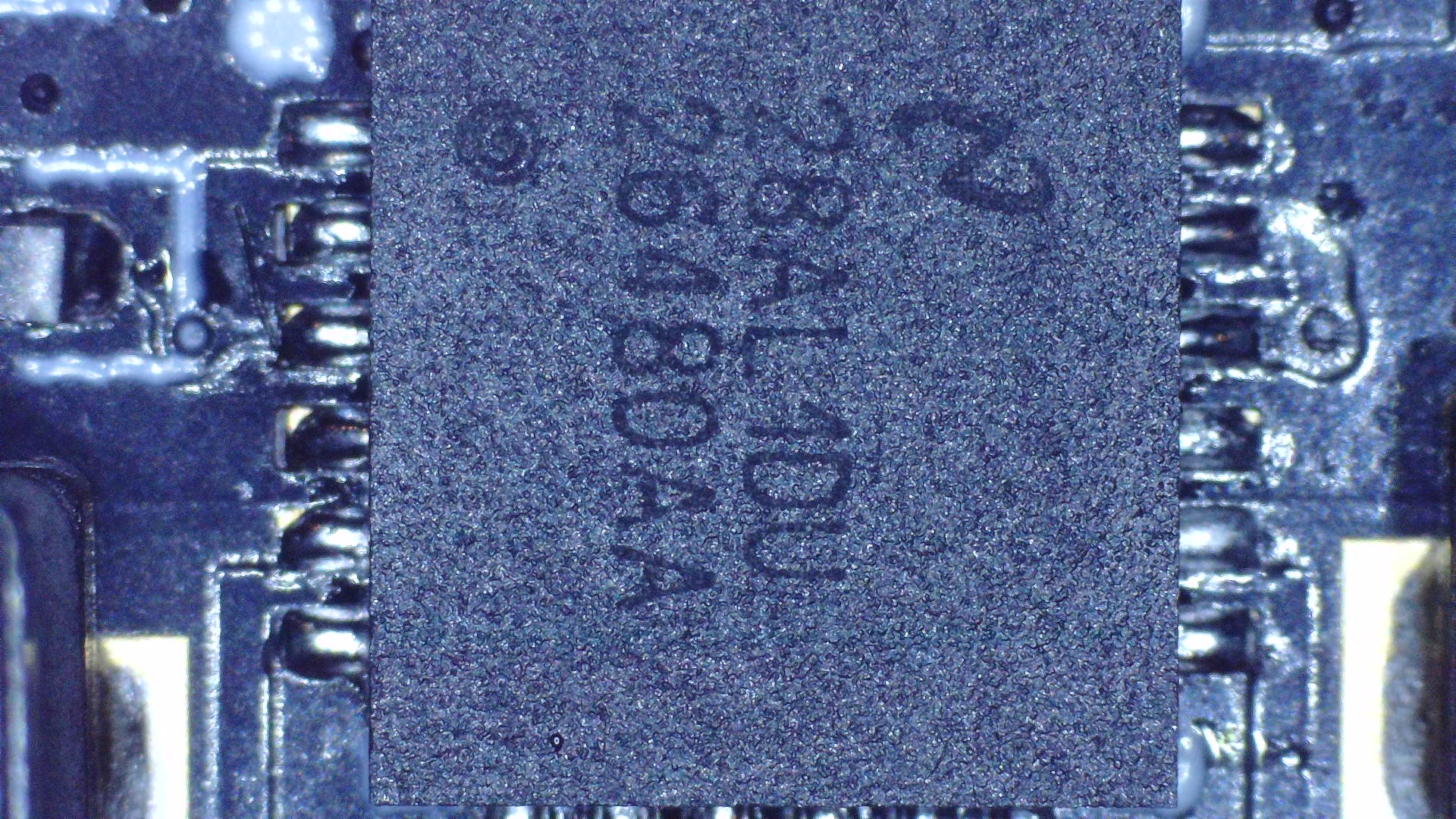
The chip to the left of the DDR3 memory is a TPS51200 sink and source DDR termination regulator. The QFN chip to the right of the DDR3 memory chip is a 26480AA buck converter from TI.
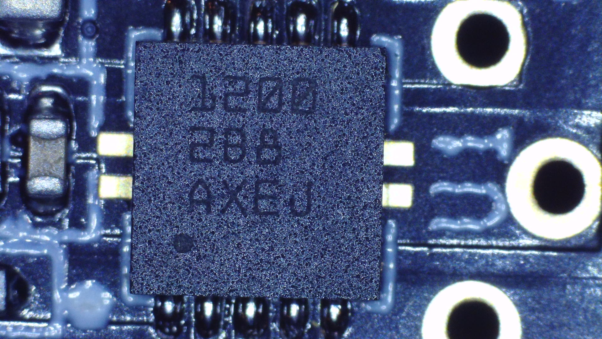
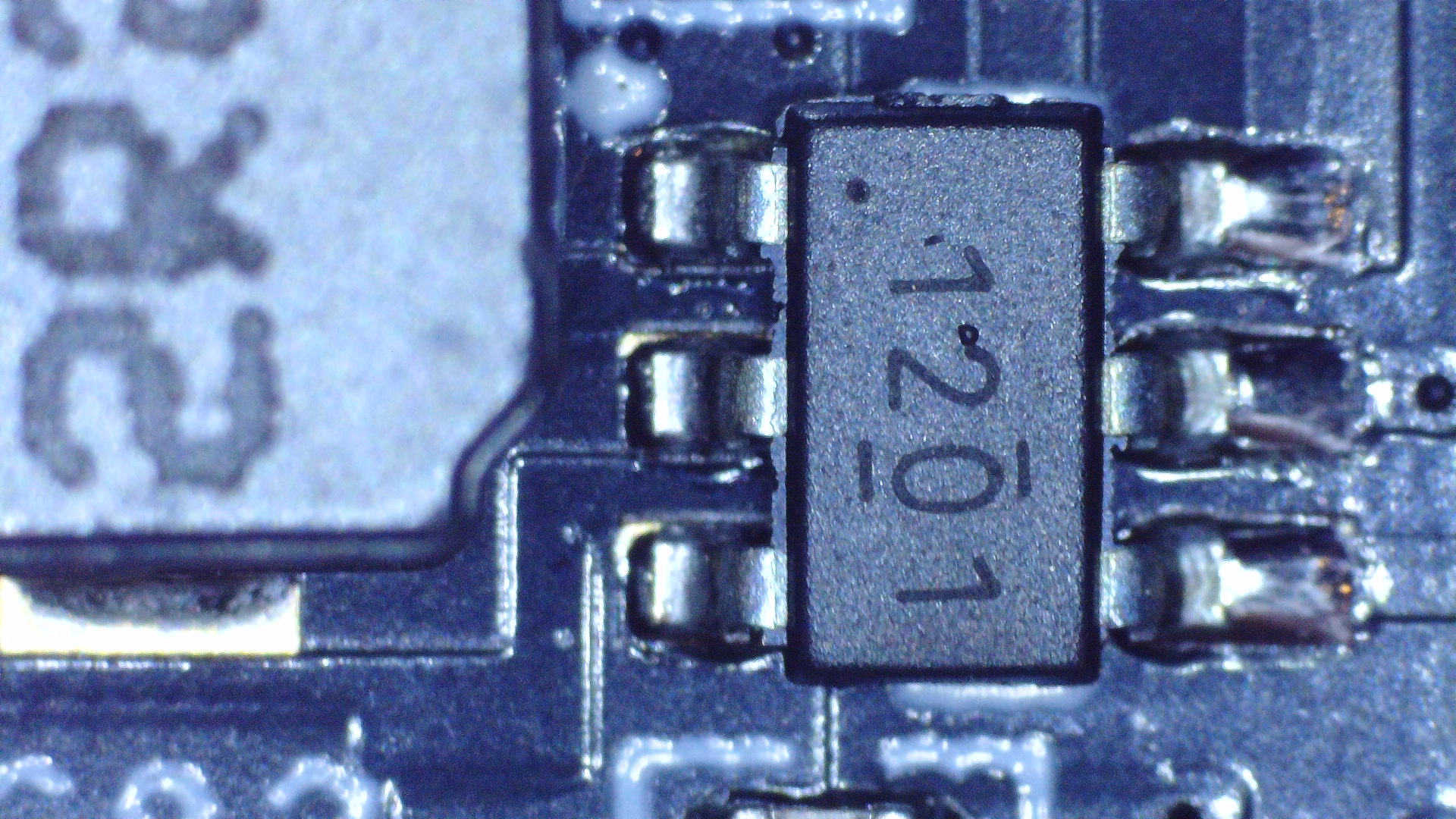
Right above the USB3 connector, there is another DC-DC converter. This one is marked 1201 and it is a TPS561201 step-down voltage regulator.
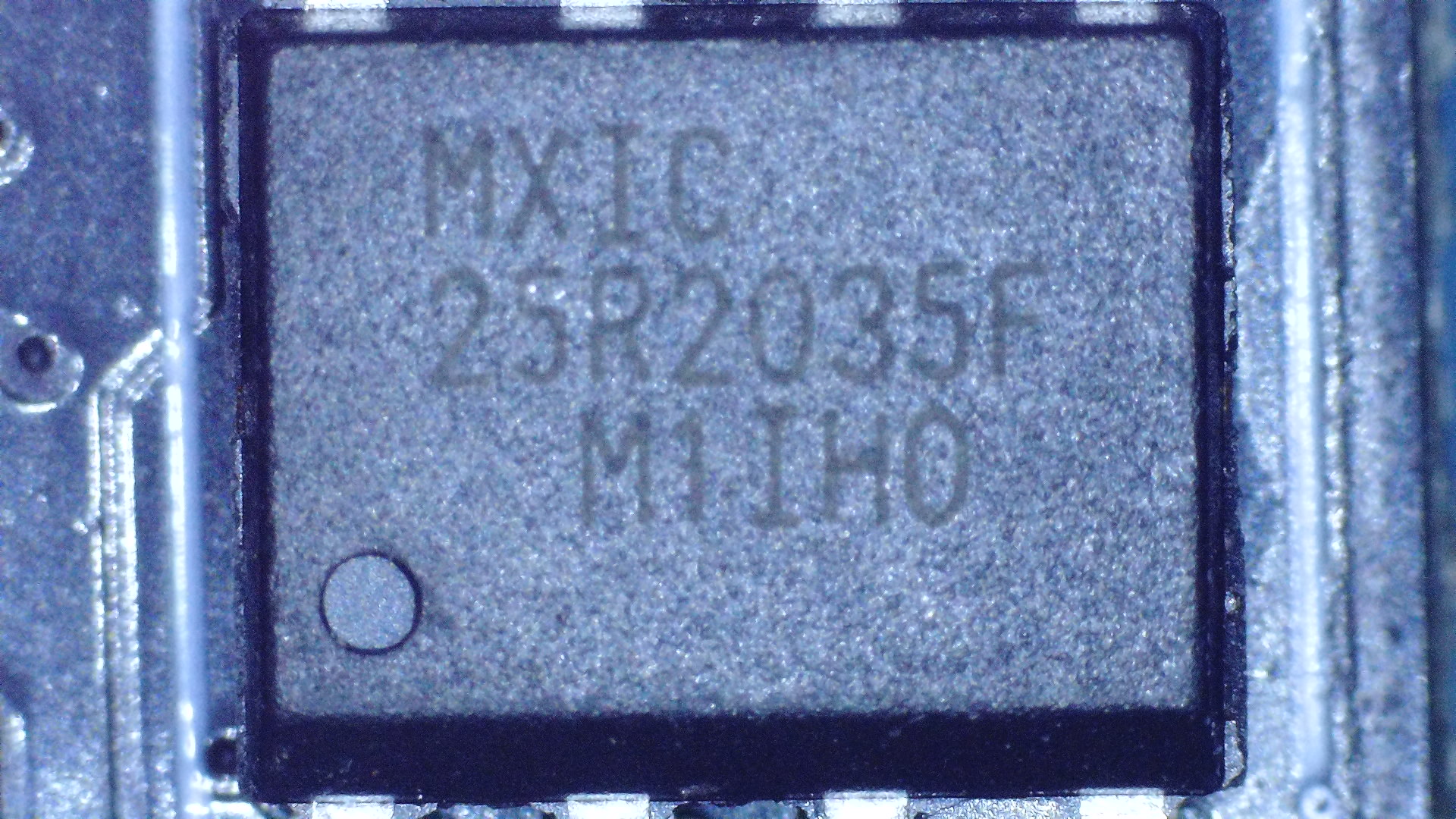
There is an 8 pin SOIC next to the JTAG header, and that is a MXIC 25R2035F 2 Mb flash memory chip.