I did a detailed review and teardown of a DreamSourceLab‘s DSTouch DS4T1012, touchscreen operated handheld oscilloscope. You can check out the review video below. In this blogpost, we are going to examine some of the teardown pictures.
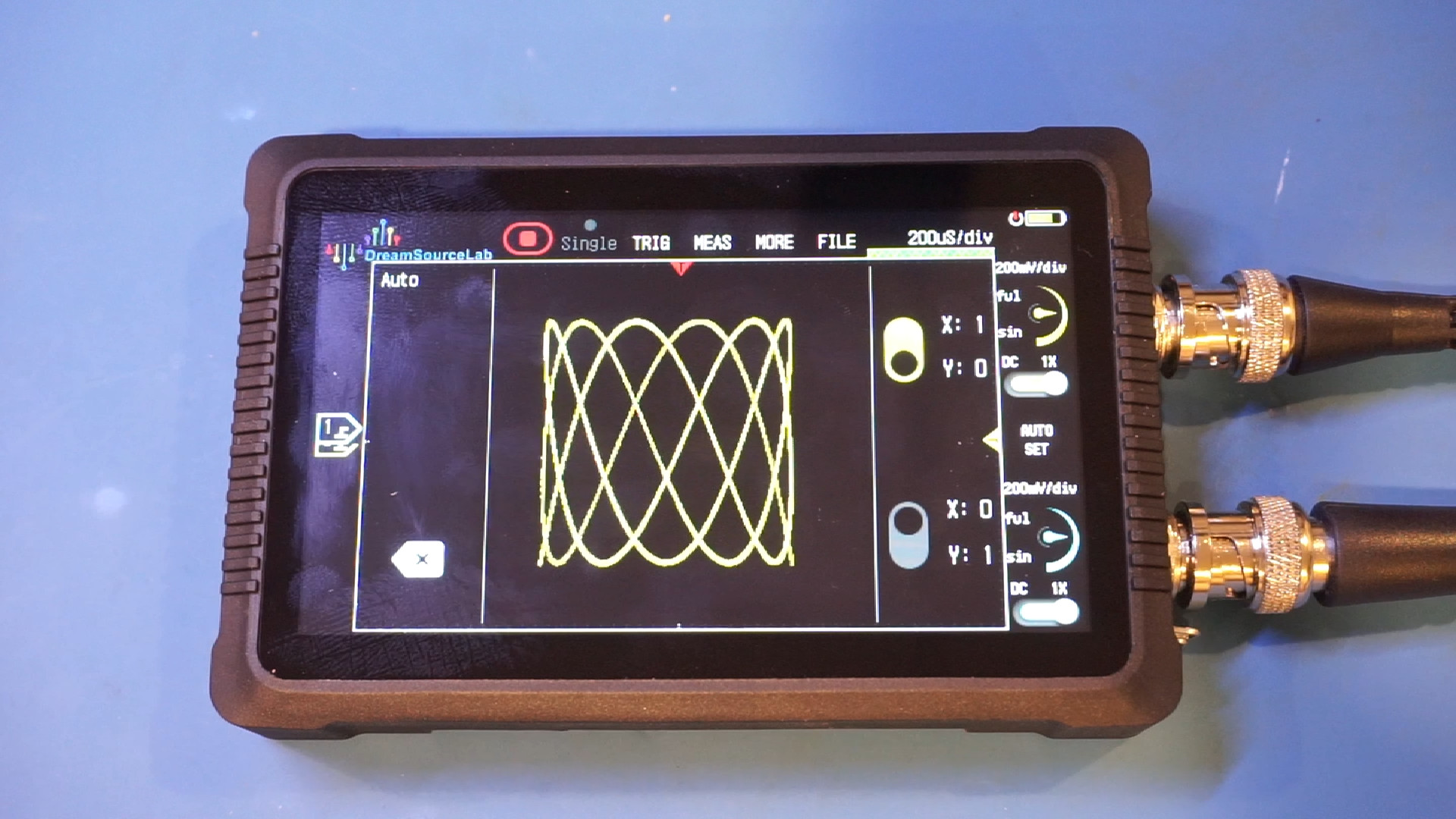
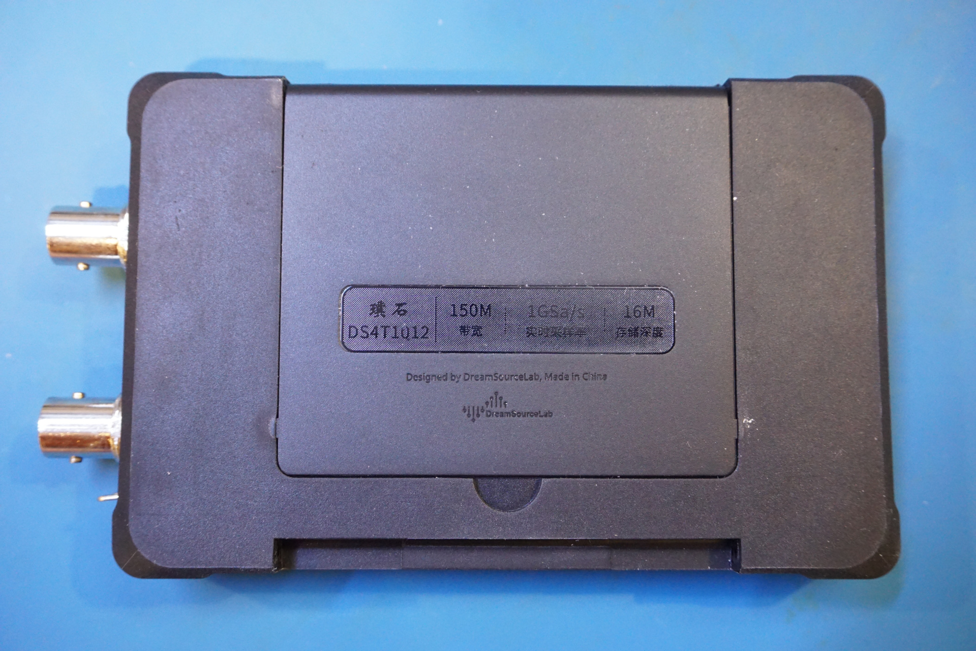
DS4T1012 is a dual channel, 150 MHz bandwidth oscilloscope. The scope has an impressive 16 Mpts memory depth, it has a builtin function generator and supports FFT analysis and real-time protocol decoding.
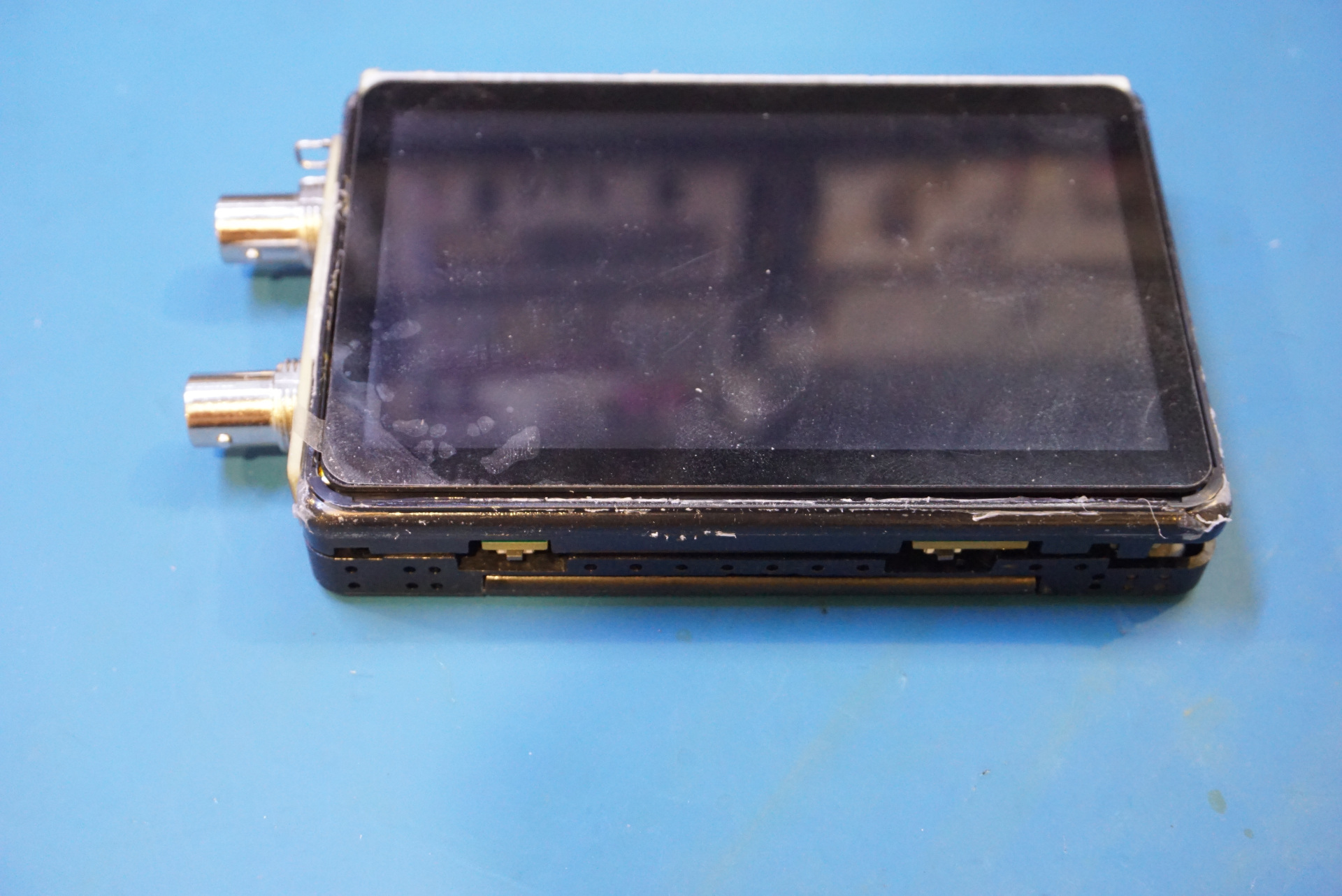
Here are a couple of pictures showing the front and the back side of the DS4T1012. There is an integrated stand on the back and it offers two tilting positions.
On the side, there is the power button and the USB-C port. The other port, according to the manual is for expansion. But DreamSourceLab currently does not have any product that can utilize this expansion port yet. Perhaps, this is planned for the future.
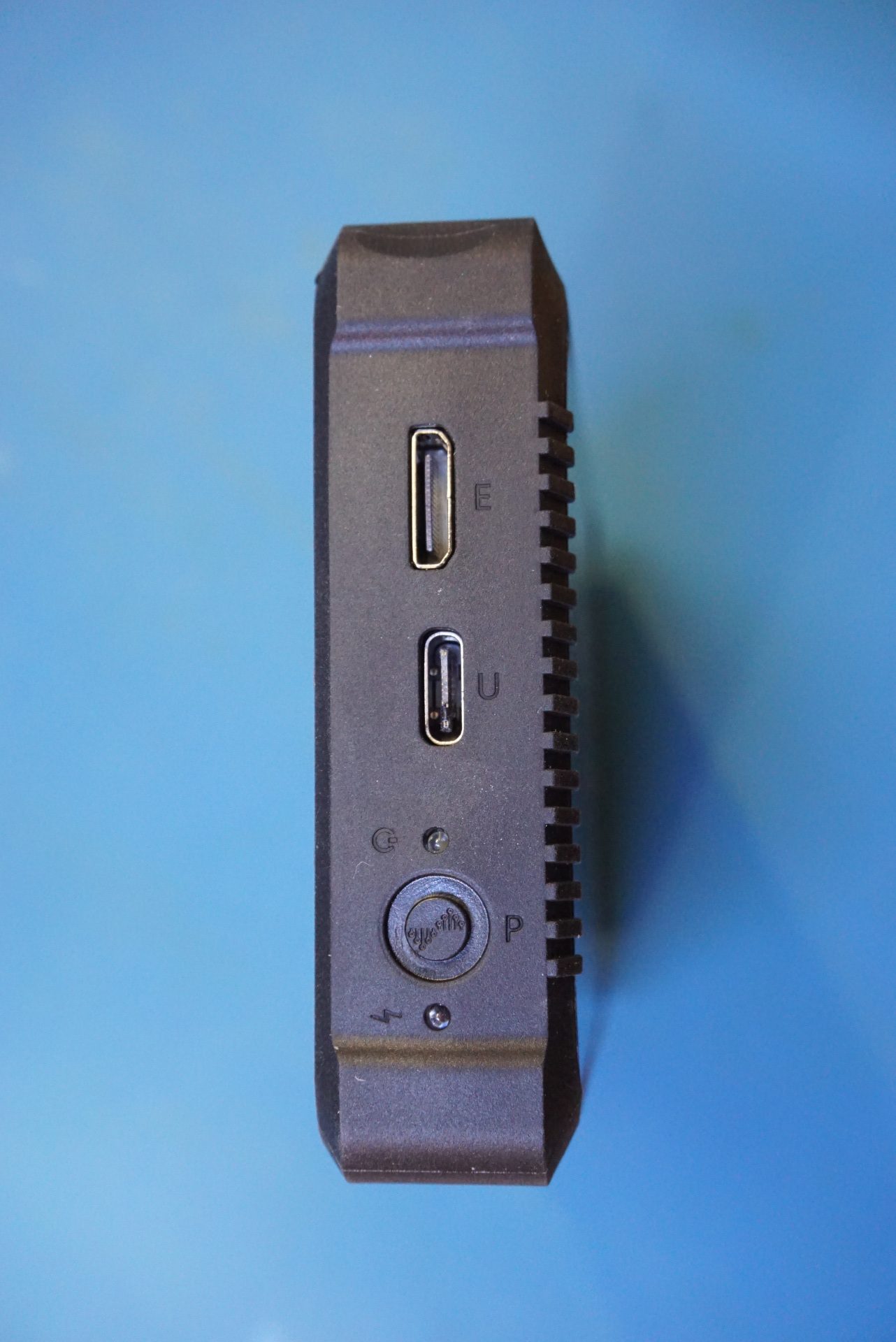
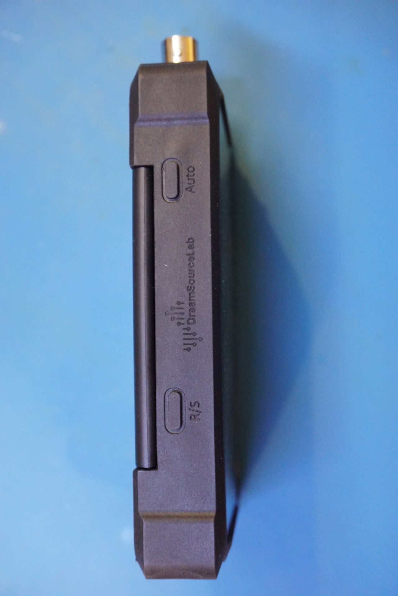
The contacts at the bottom of the case are for external charging dock. Again, I have not seen any charging accessories for the DS4T1012 on DreamSourceLab’s website. Because the scope is operated by the touch screen, it only has a couple of buttons on the top side. One is for run and stop the other is for auto acquisition.
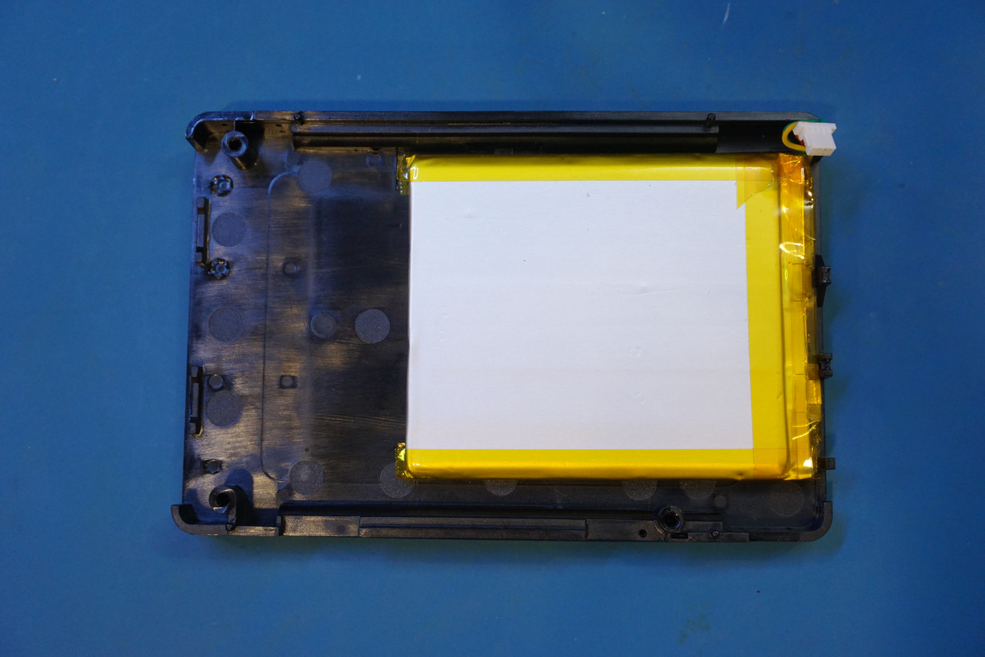
One thing a little bit of unusual is that the rubber holster is actually part of the structural element that holds the DS4T1012 together. Once the rubber holster is removed, you can see that the circuit board is essentially sandwiched between the LCD screen and the bottom half of the case and there are no screws securing these pieces into place. (You can see this more clearly in the teardown video linked at the beginning of this post).
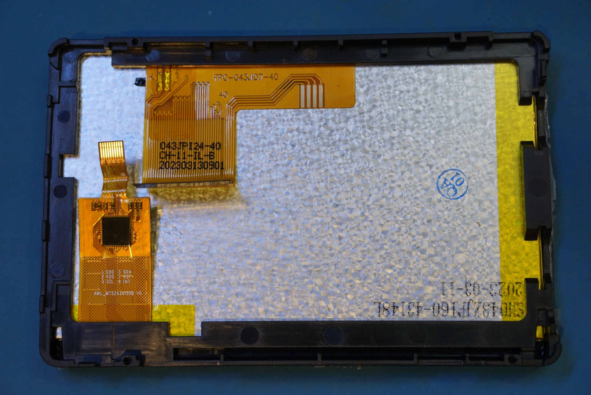
There is a fairly large Lipo battery cell mounted on the back. The exact runtime figure has not been published, but in my testing, the battery level only dropped by 1/3 after a couple of hours of continuous use. So a single charge should get you through most of the day without any problem. To the right you can see the LCD screen with the builtin touch controller.
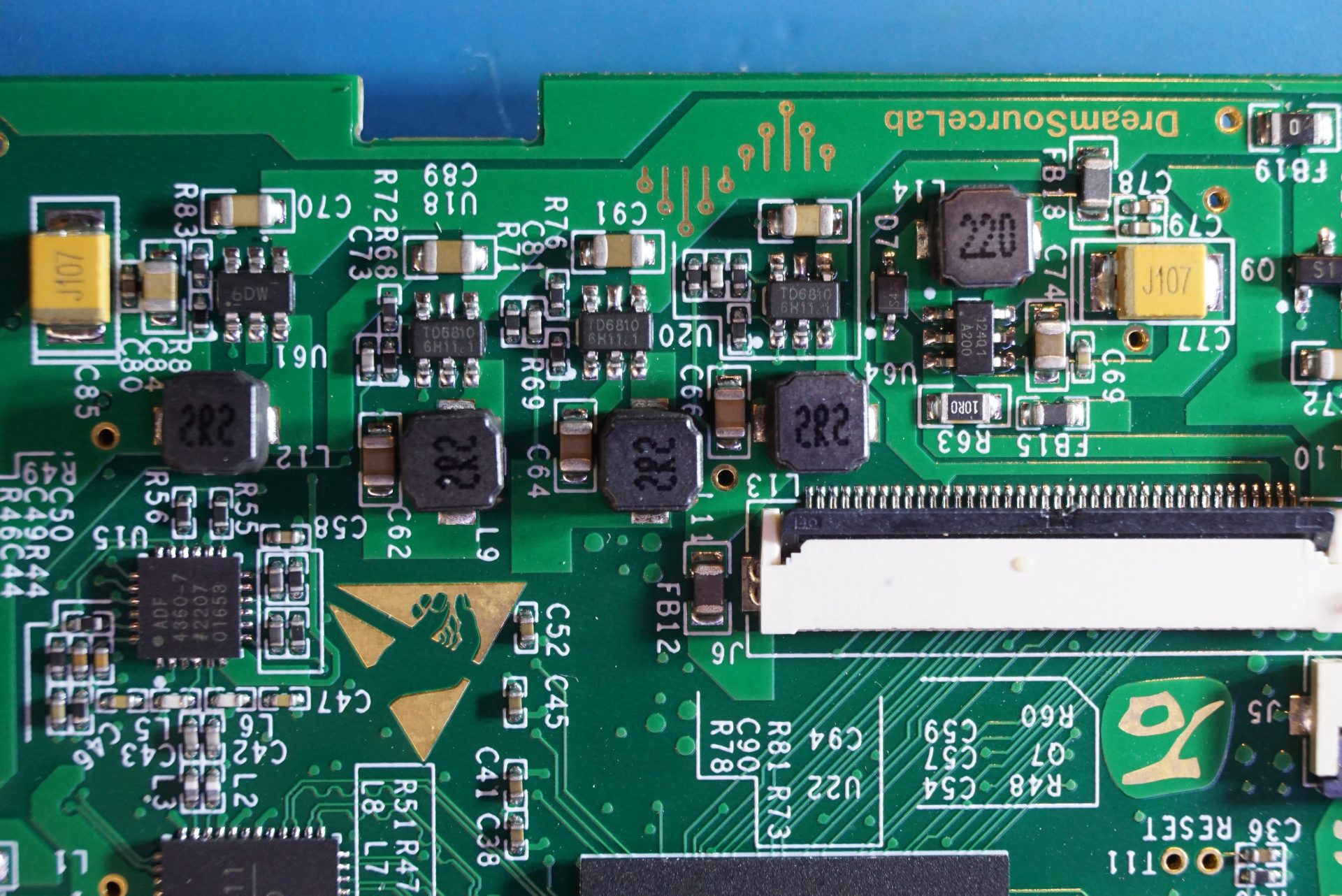
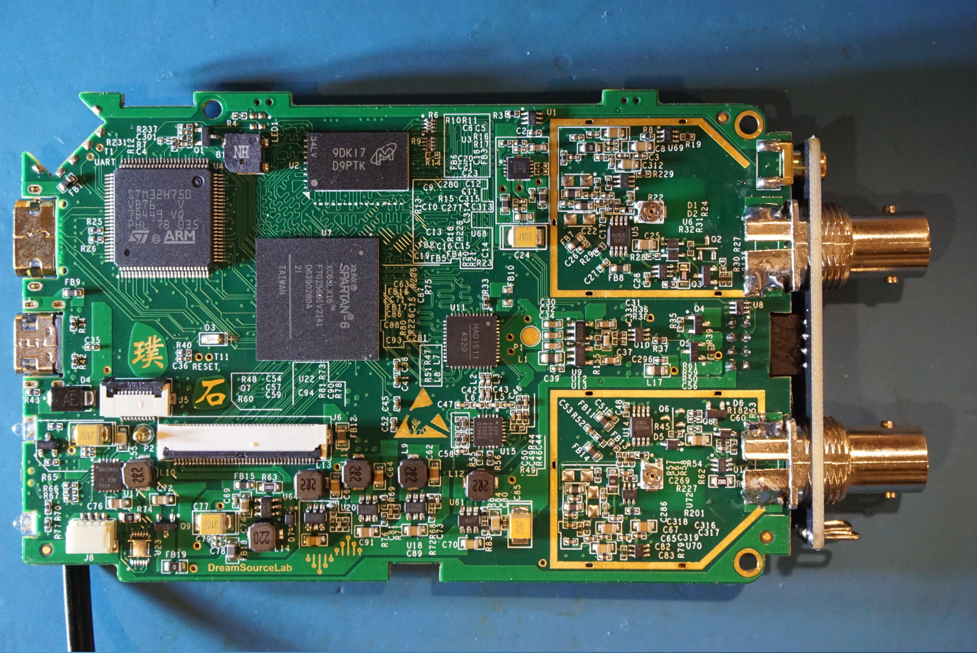
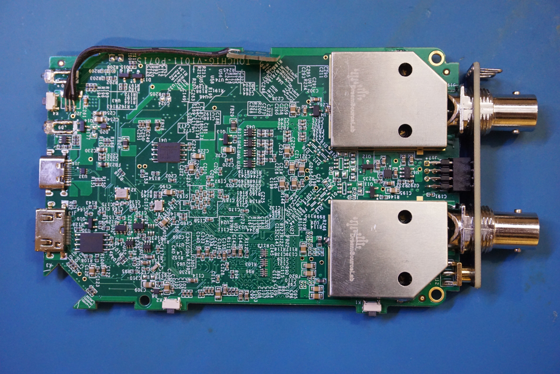
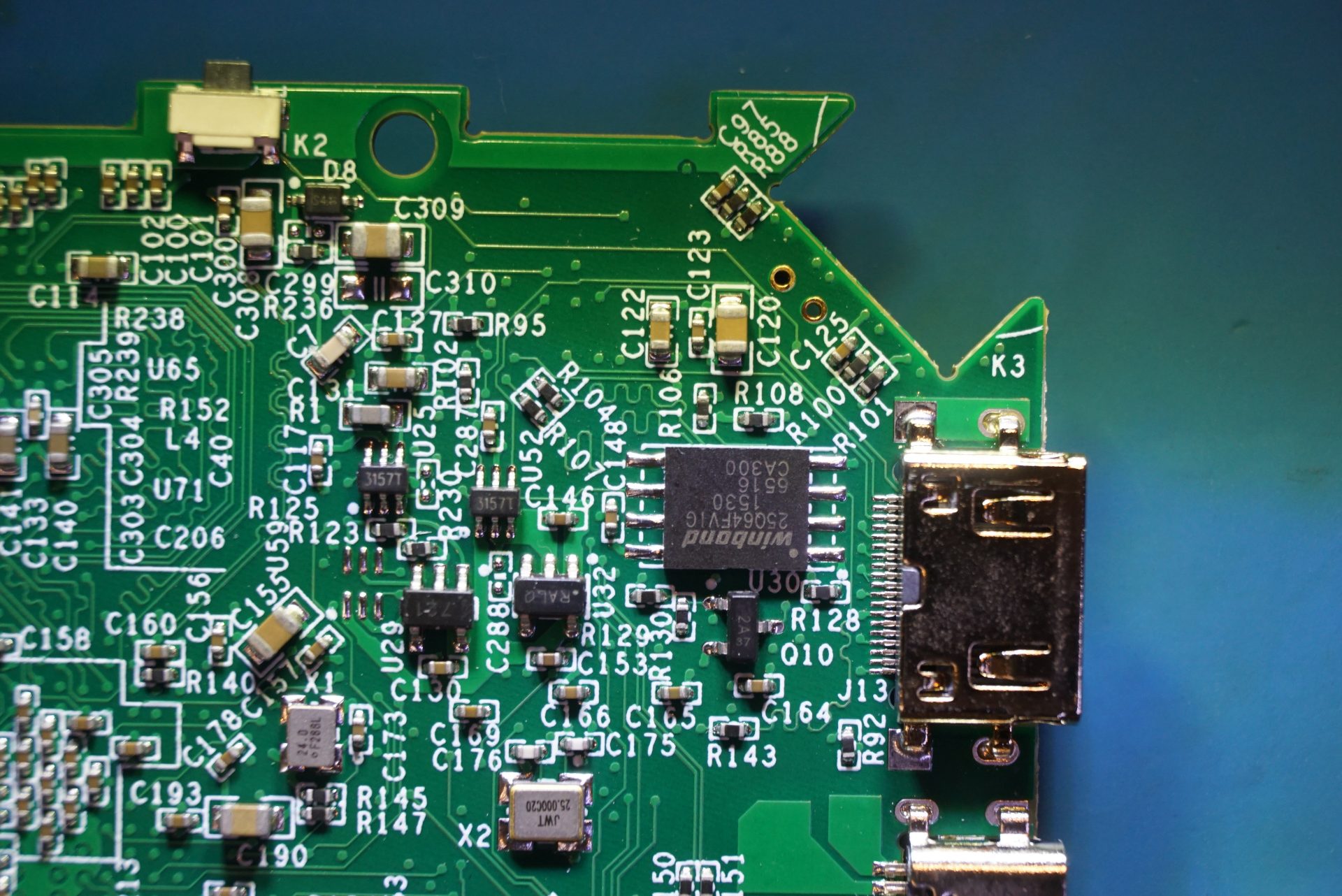
Here is a picture of the main circuit board. Each section is further explained later in the article.
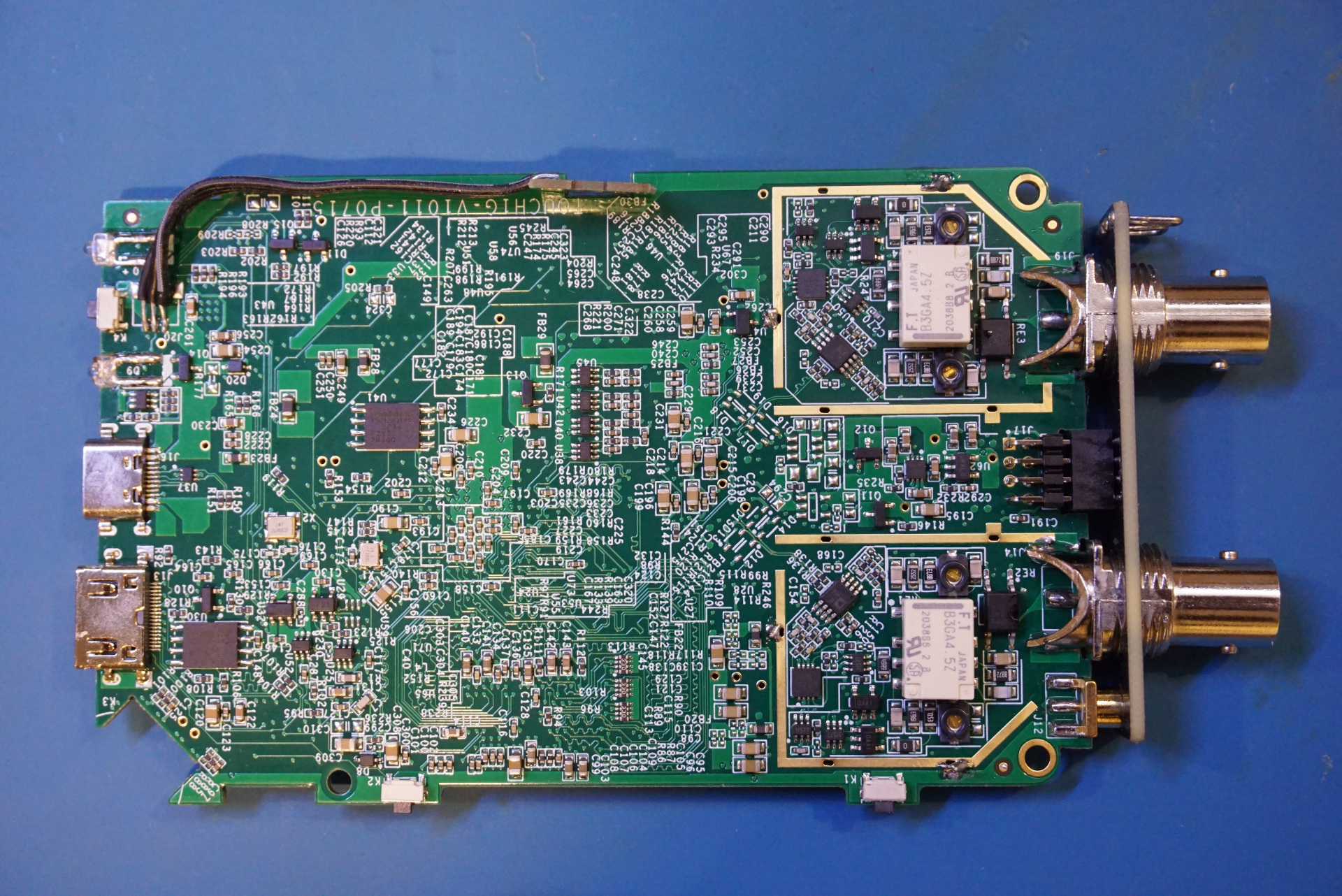
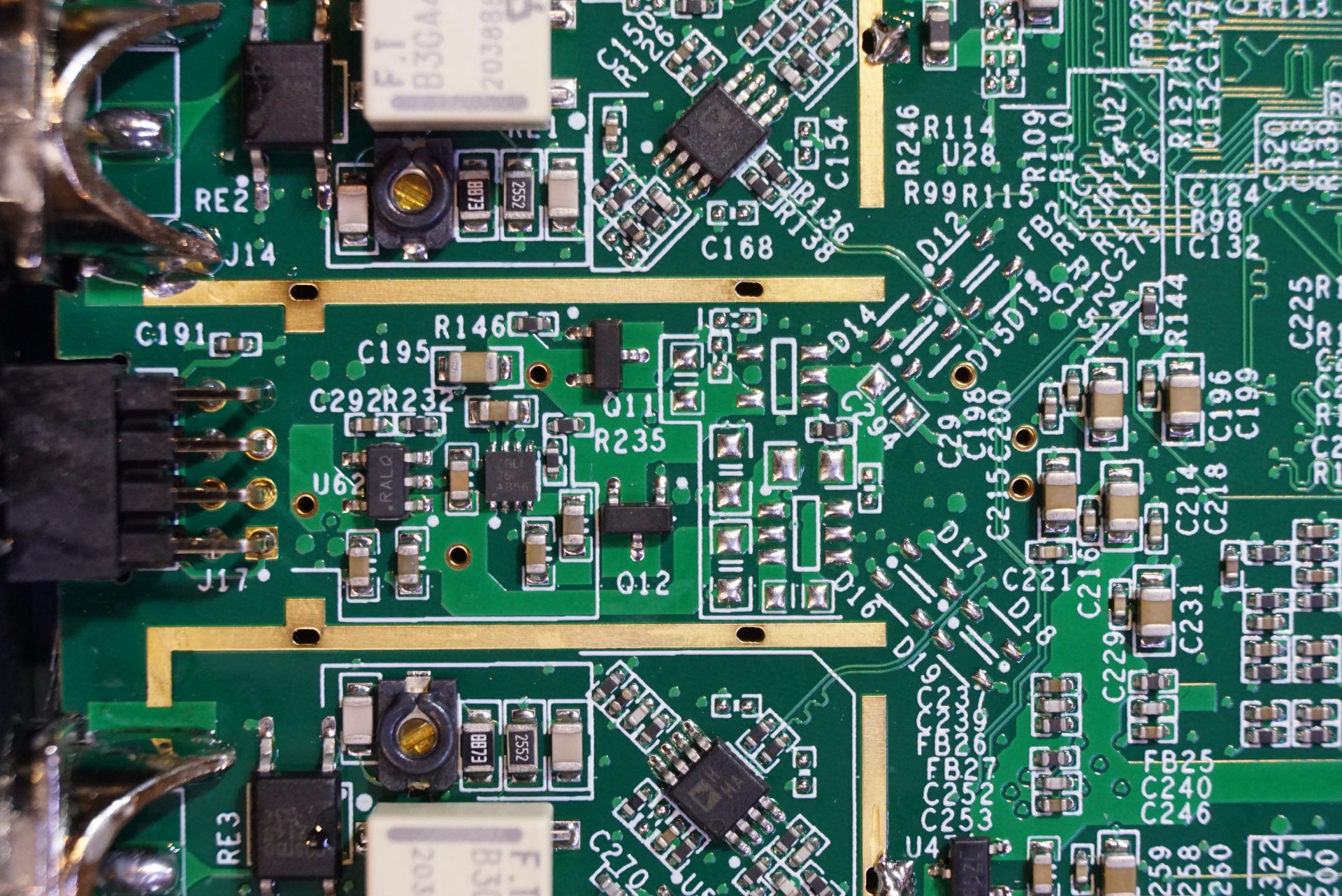
Here are a couple of pictures of the reverse side of the PCB. The input sections are shielded. In the picture to the right below, the input shielding cans had been removed.
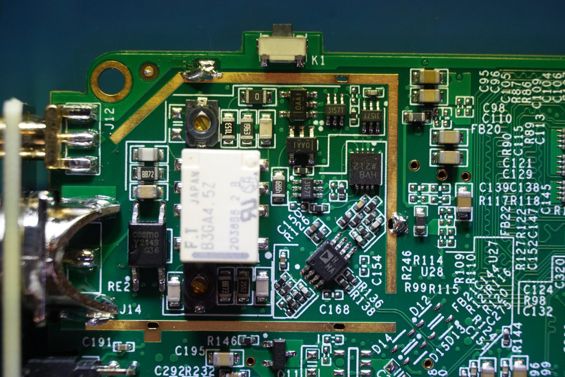
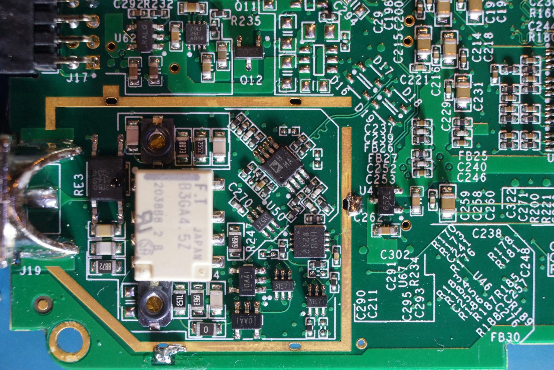
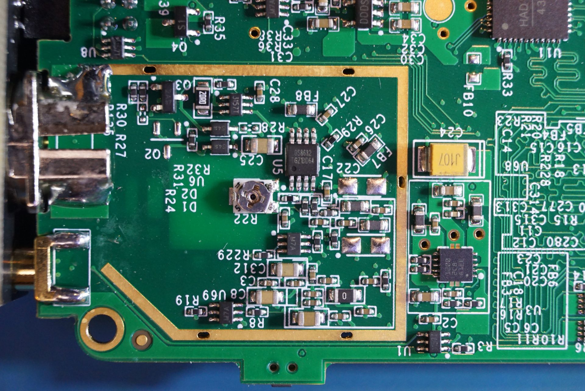
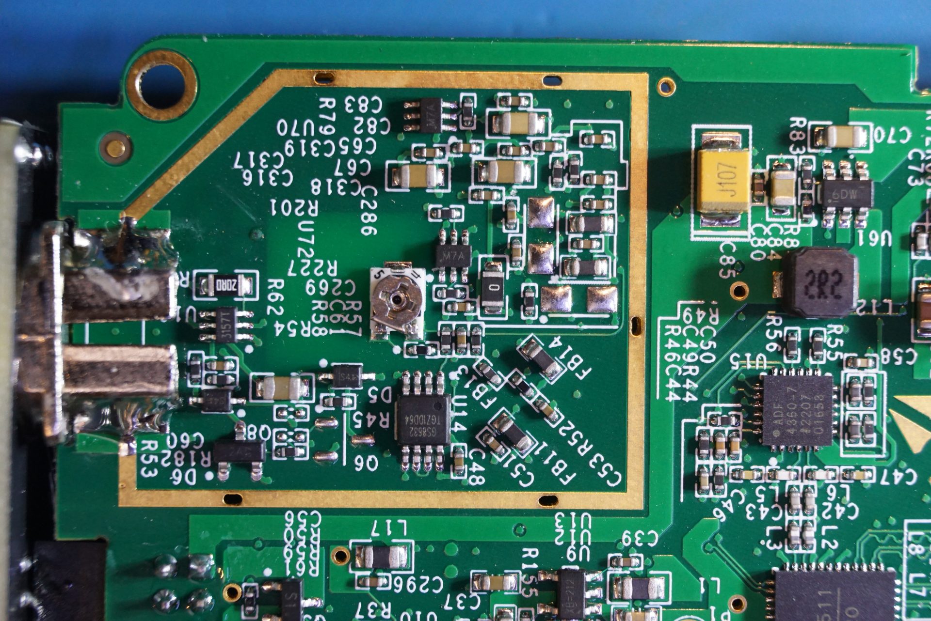
Here are a couple of pictures showing the channel 1 and channel 2 input sections. The picture to the left is channel 1 and the picture to the right is channel 2. For each of the channels, there is a solid sate relay and a mechanical relay for range switching. Unfortunately, I did not recognize most of the SMD markings.
The pictures below are the input sections on the other side of the board. Again, the picture to the left is channel 1, and the picture to the right is channel 2. There are some slight differences between these two channels. Channel 2 has a few more components compared to channel 1. The Opamp used here is GS8532, a rail-to-rail Opamp with builtin anti-EMI RF filter.
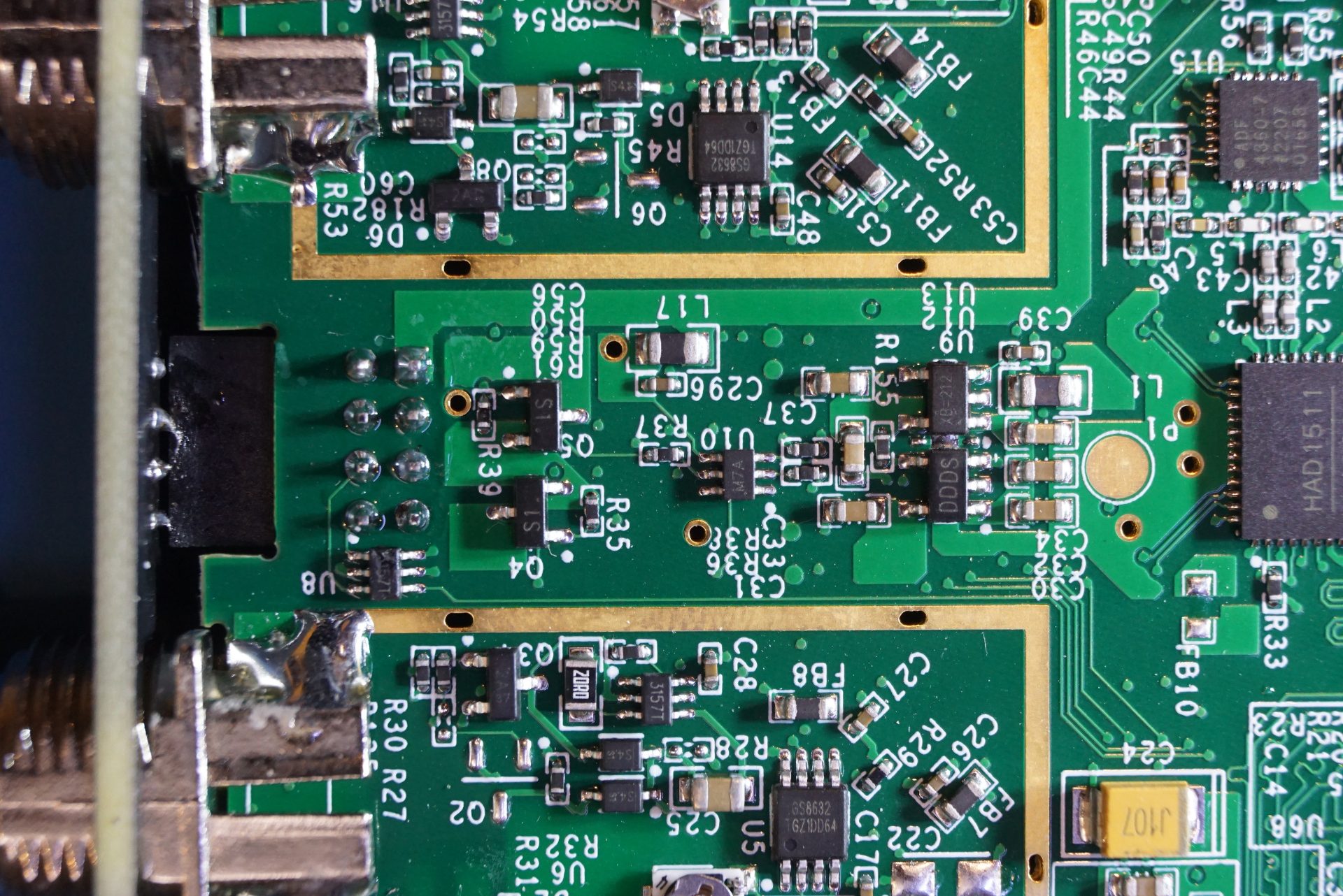
Here are a couple of pictures showing the section of the circuitry in between the two input channels on either side of the board.
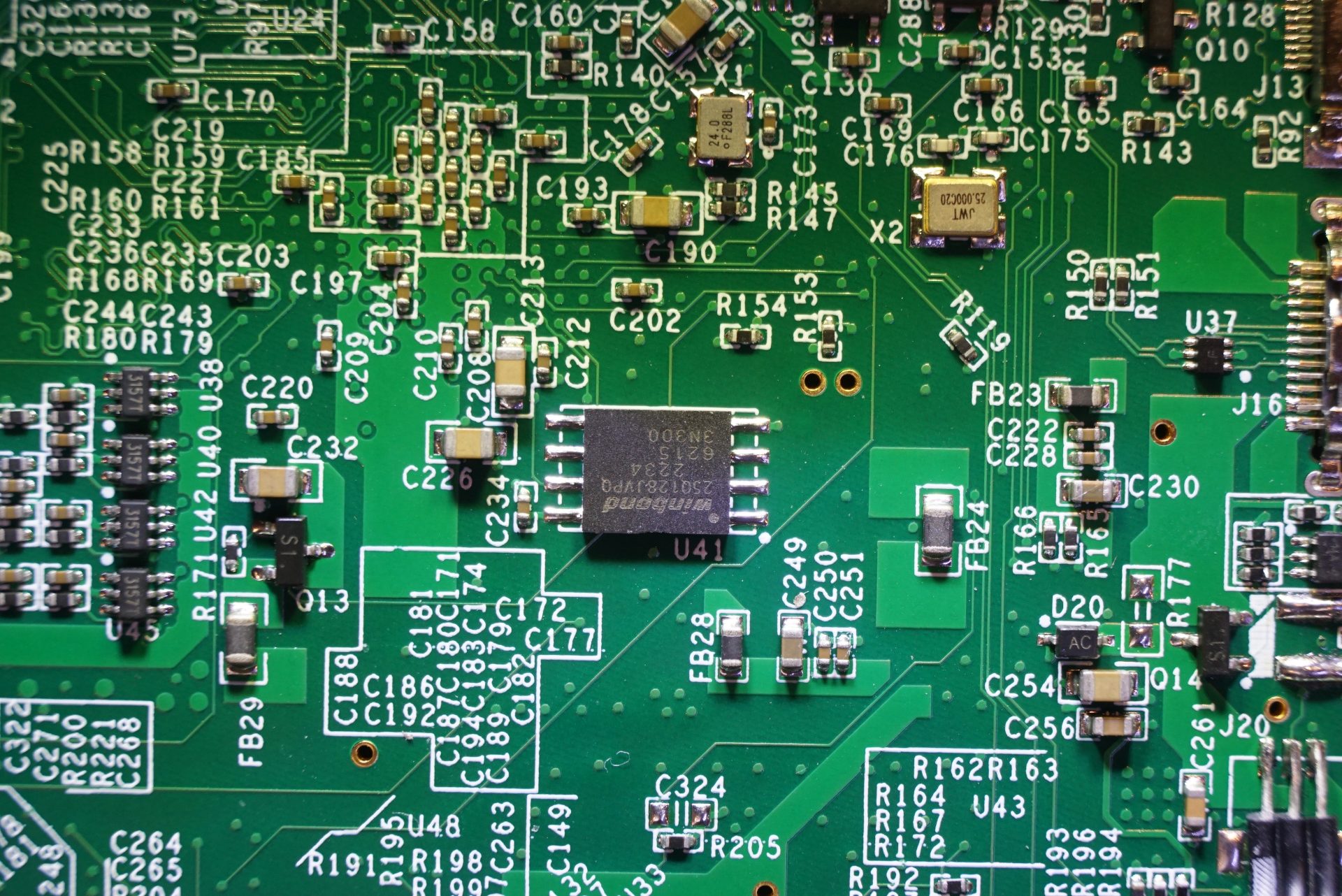
There are a couple of windbond flash memory chips on the reverse side of the PCB. One is 64 MB, the other is 128 MB.
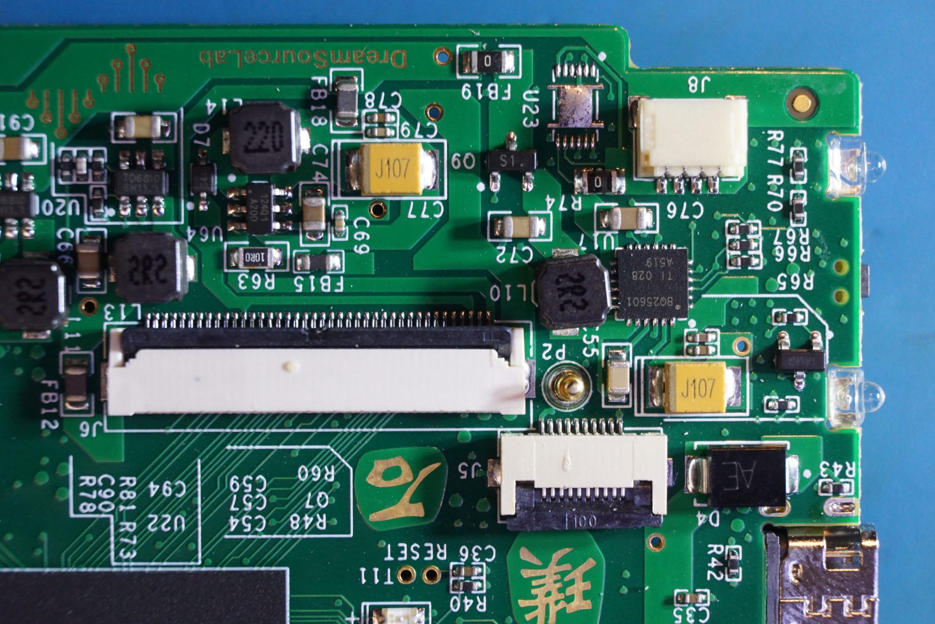
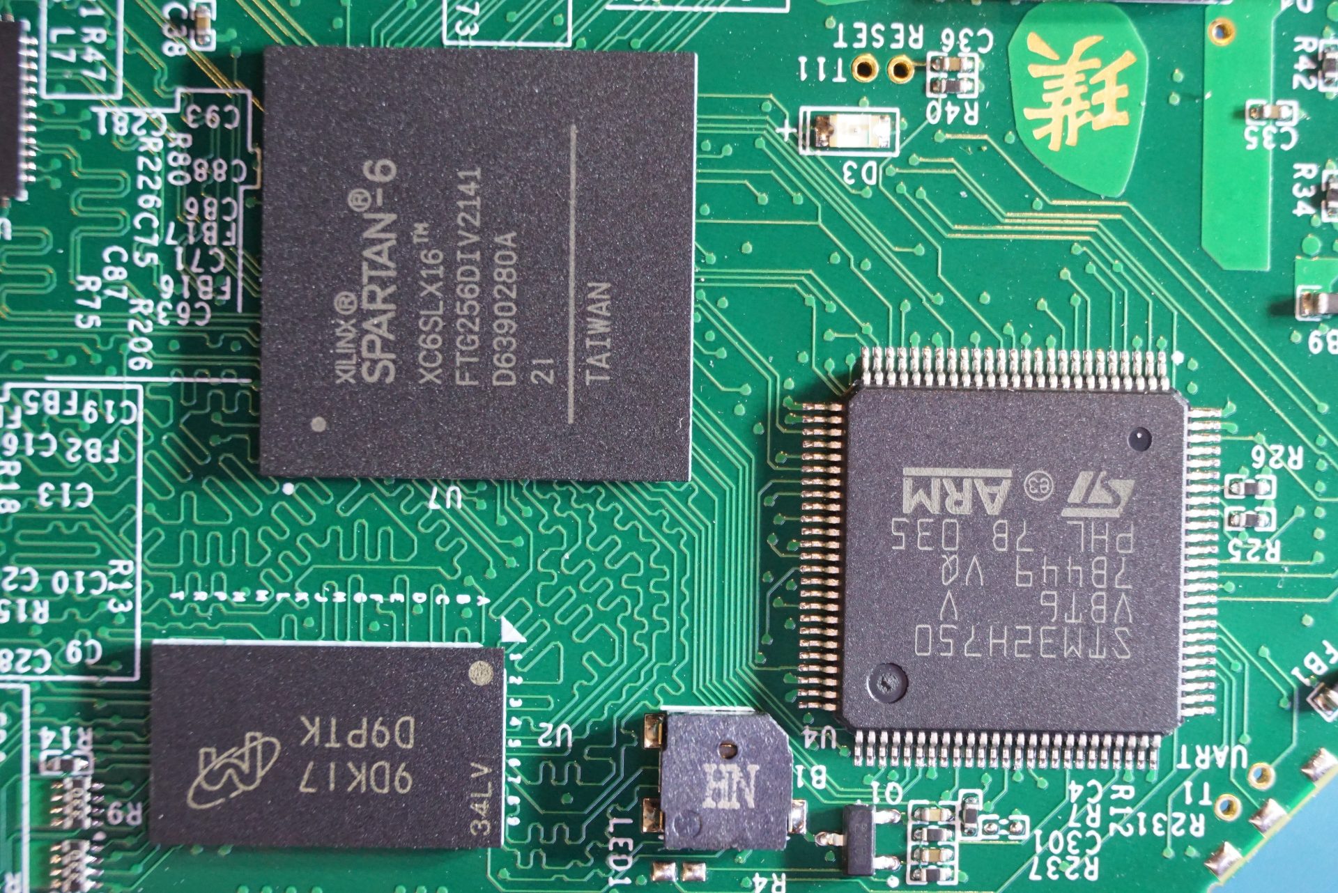
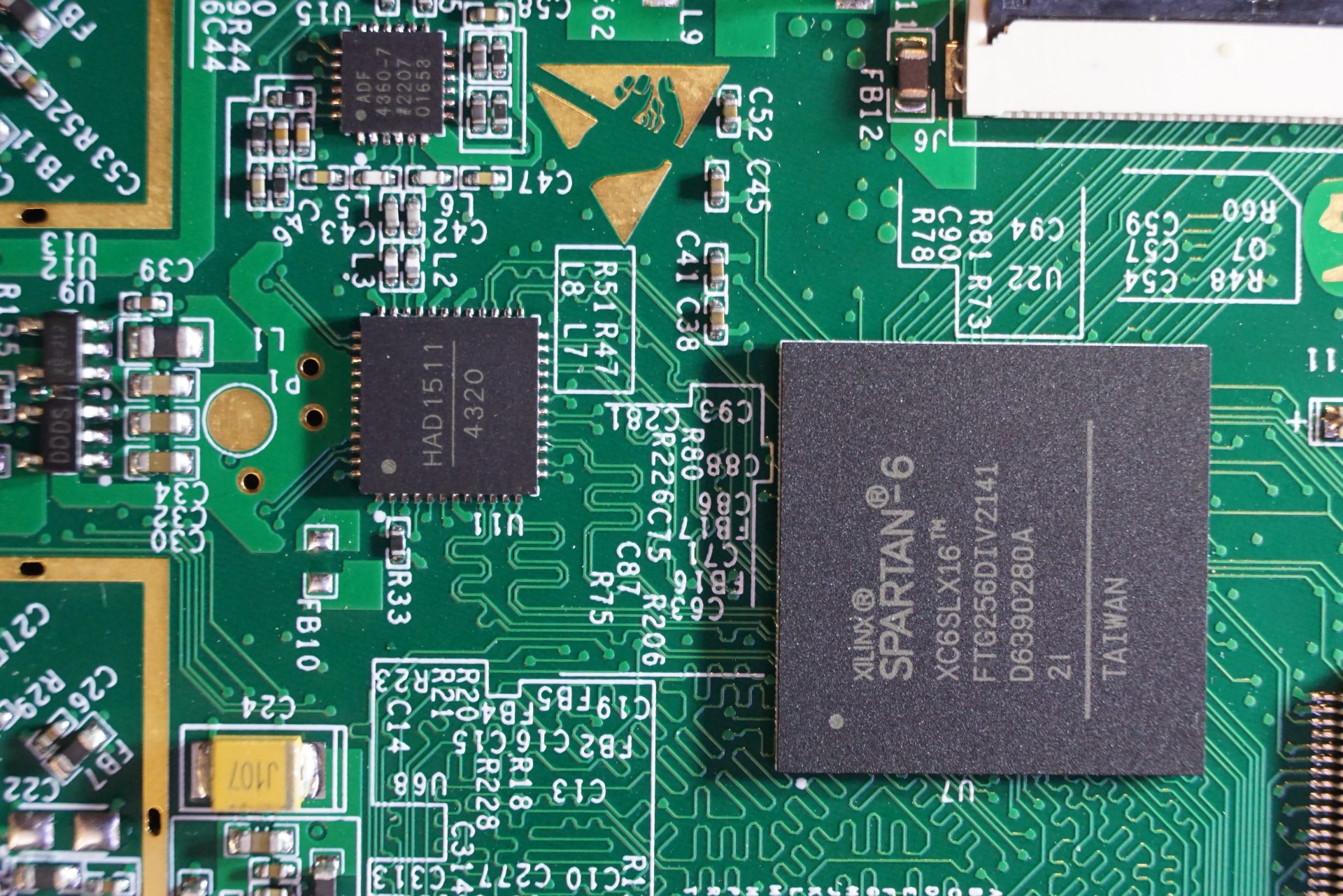
The FPGA used in the DS4T1012 is a XLINX SPARTAN-6 family FPGA. This is a rather powerful FPGA and it has 14,579 logic cells. The sample memory (16Mpts) is implemented in the DRAM. You can see the DRAM chip in the picture to the left below. The MCU used is an STM32H750 microcontroller.
To support the 1GSa/s sampling rate, an HAD1511 ADC is used. We have seen this ADC used in many handheld oscilloscopes, including both the OWON HDS272S and the OWON HDS2102S I had reviewed before. The ADF4360-7 synthesizer and VCO is used to generate the clock for the HAD1511. You can clearly see the two input coupling capacitors next to pin 35 and 36 of the HAD1511. These two pins are for the clock inputs.
In the picture to the left below you can see the DC-DC converter section. This section is responsible for generating the voltage rails needed by the FPGA. Multiple TD6810‘s (synchronous step-down DC-DC converter) are used here. The battery charging section can be found In the image to the right below, a BQ25601 charger chip is used.