Over the last couple of weeks, I did a few videos on the new UNI-T UPO1204 200 MHz 4 channel digital oscilloscope. In this blog post, let’s take a look at some of the teardown pictures.
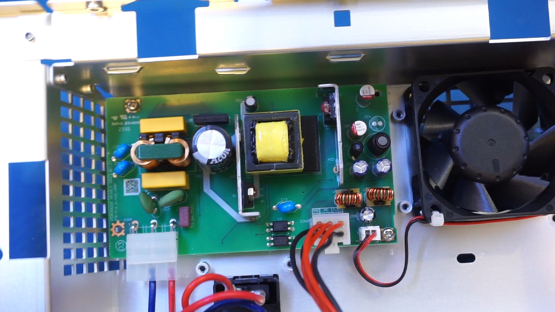
The case is well shielded. Mounted on the back cover is a rather minimalist power supply module. The cooling fan is connected to the power supply direct and is always on unfortunately whenever the hardware power switch is switched to the on position even when the oscilloscope is on standby. The fan is relatively quite but it would be nice is the fan is switched off in standby mode.
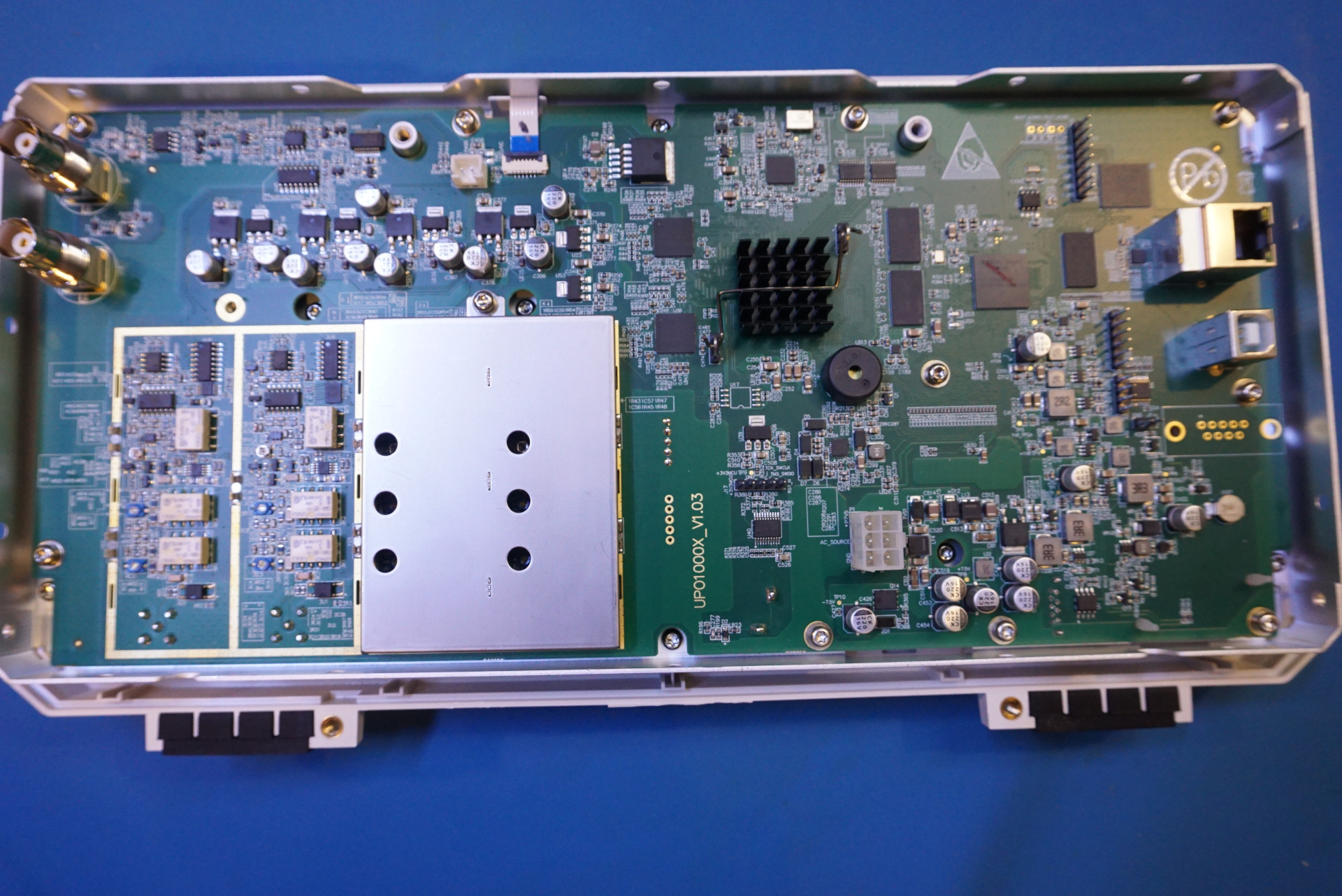
Here is a picture of the main PCB with the channel one and two input shielding can removed.
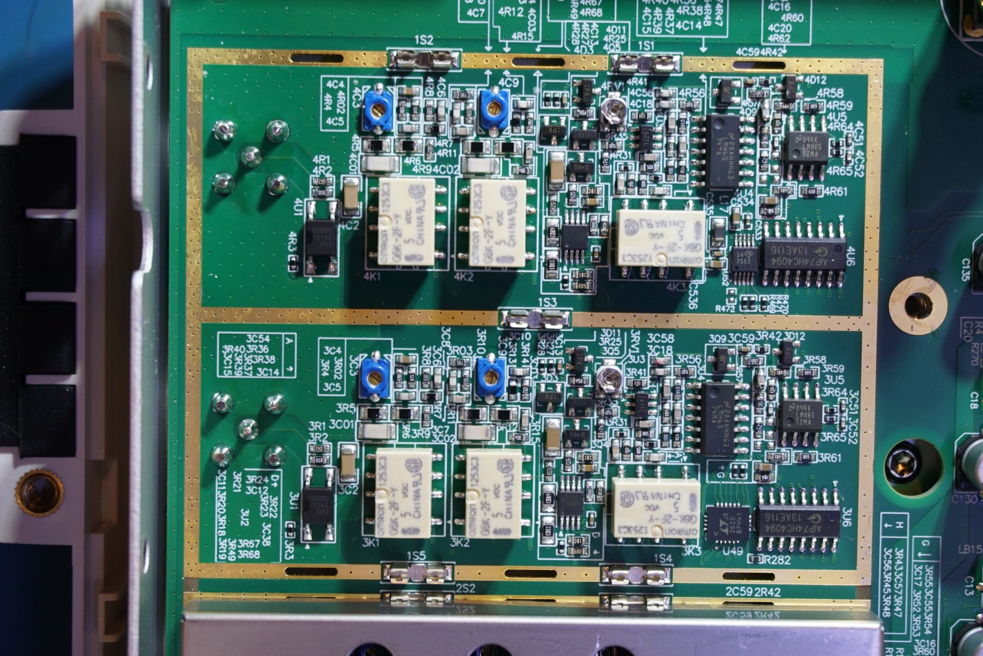
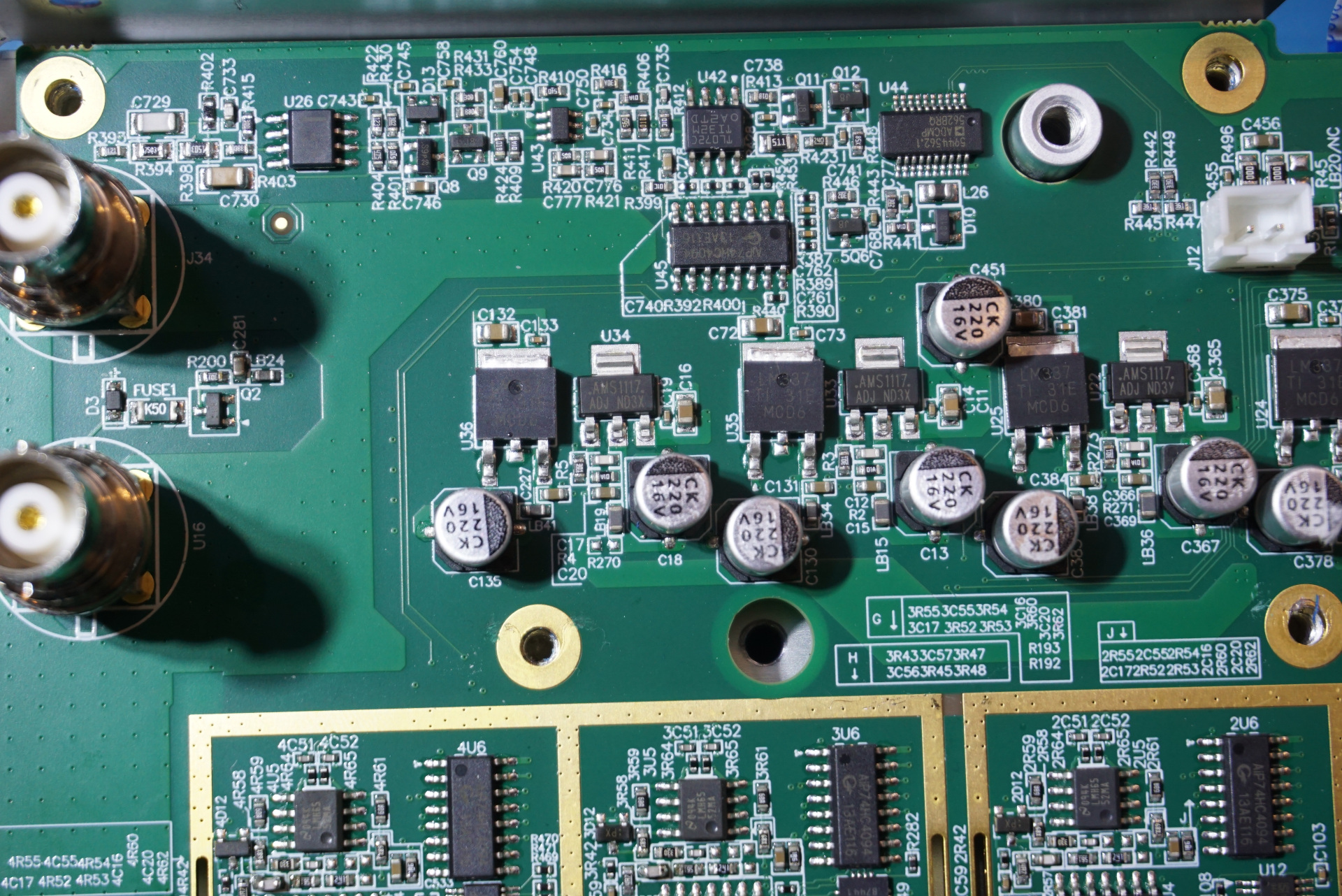
Here is close-up picture of the four input sections with the shielding cans removed:
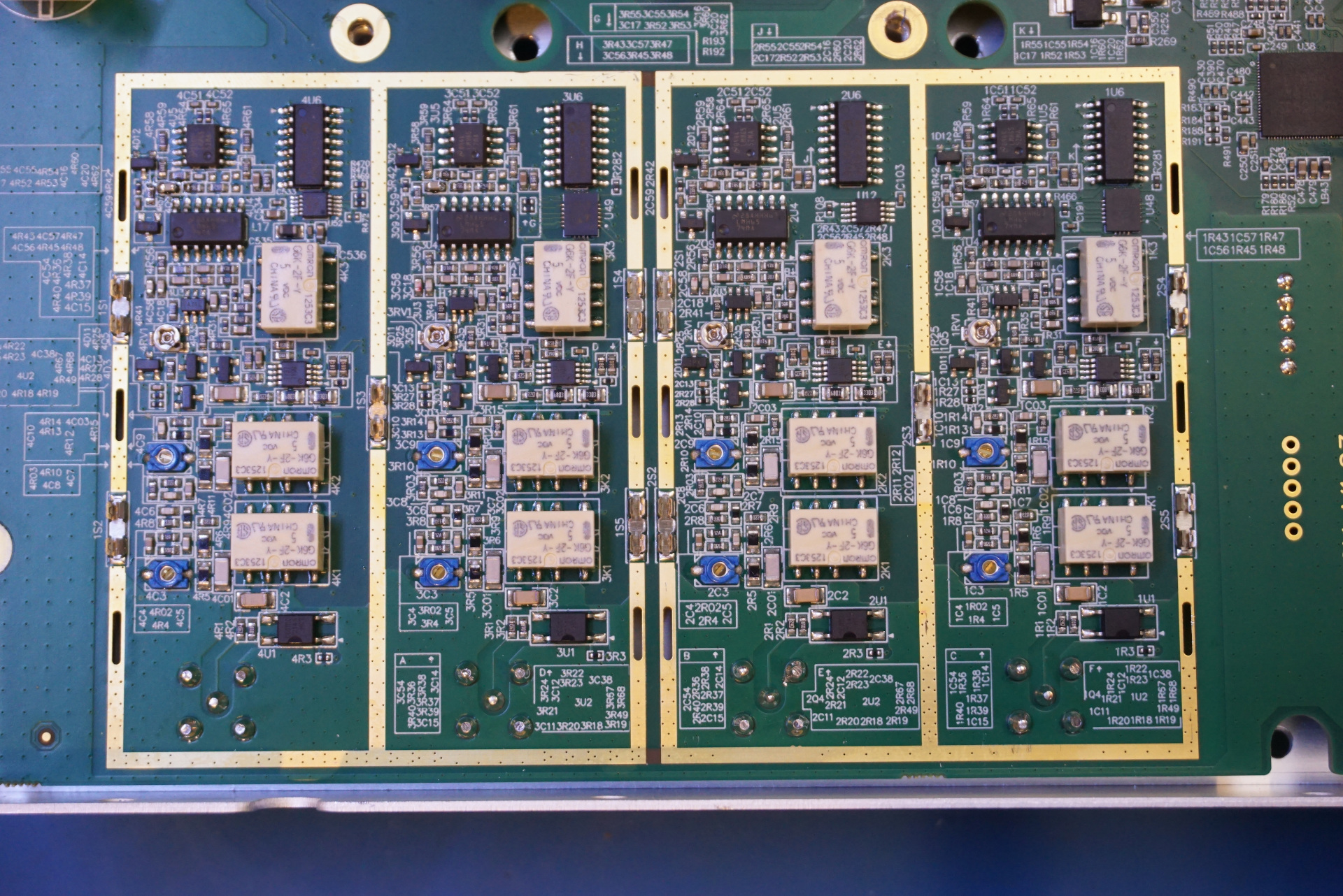
There are some minimal circuitry on the reverse side of the PCB but I could not fully remove the main PCB from the casing. Each channel has a COSMO Y214S solid state relay, a LMH6574 high speed video mutiplexer and a LM6552 1.5 GHz high speed differential amplifier.
Each channel has a 74HC4094 shift register. Each channel also has a DAC, presumably it is used to set amplifier gains. The DAC used in channel 1 and channel 3 is LT2620, an octal 12-bit rail-to-rail DAC. And the DAC used in channel 2 and channel 4 is DAC7562, a dual 12-bit DAC.
There are a larger number of linear regulators right above the input section. Towards the upper right there is an ADCMP562BRQ high speed comparator.
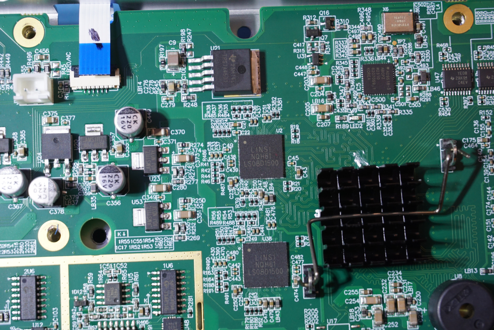
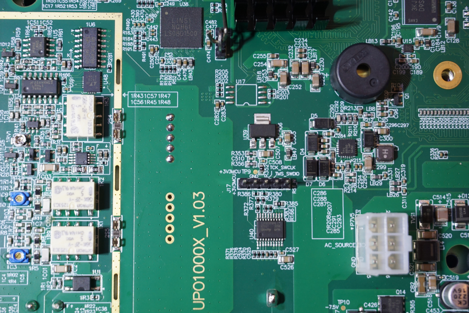
Towards the top middle in the picture below, you can see another LDO TPS7A4501. The main ADCs used in the UPO1204 are two LS08D1500, these are dual 8-bit 1.5 GSa/s ADC. These are very likely to be interleaved to support the 2GSa/s rated sampling rate given the sampling rate characteristics as the number of channels increases (2GSa/s for a single channel, 1GSa/s for two channels and 500 MSa/s for three and four channels).
The clock generator used is an AD9518. To the right of the clock generator are two YE08 bidirectional voltage level translators. I didn’t remove the heat sink from the main FPGA.
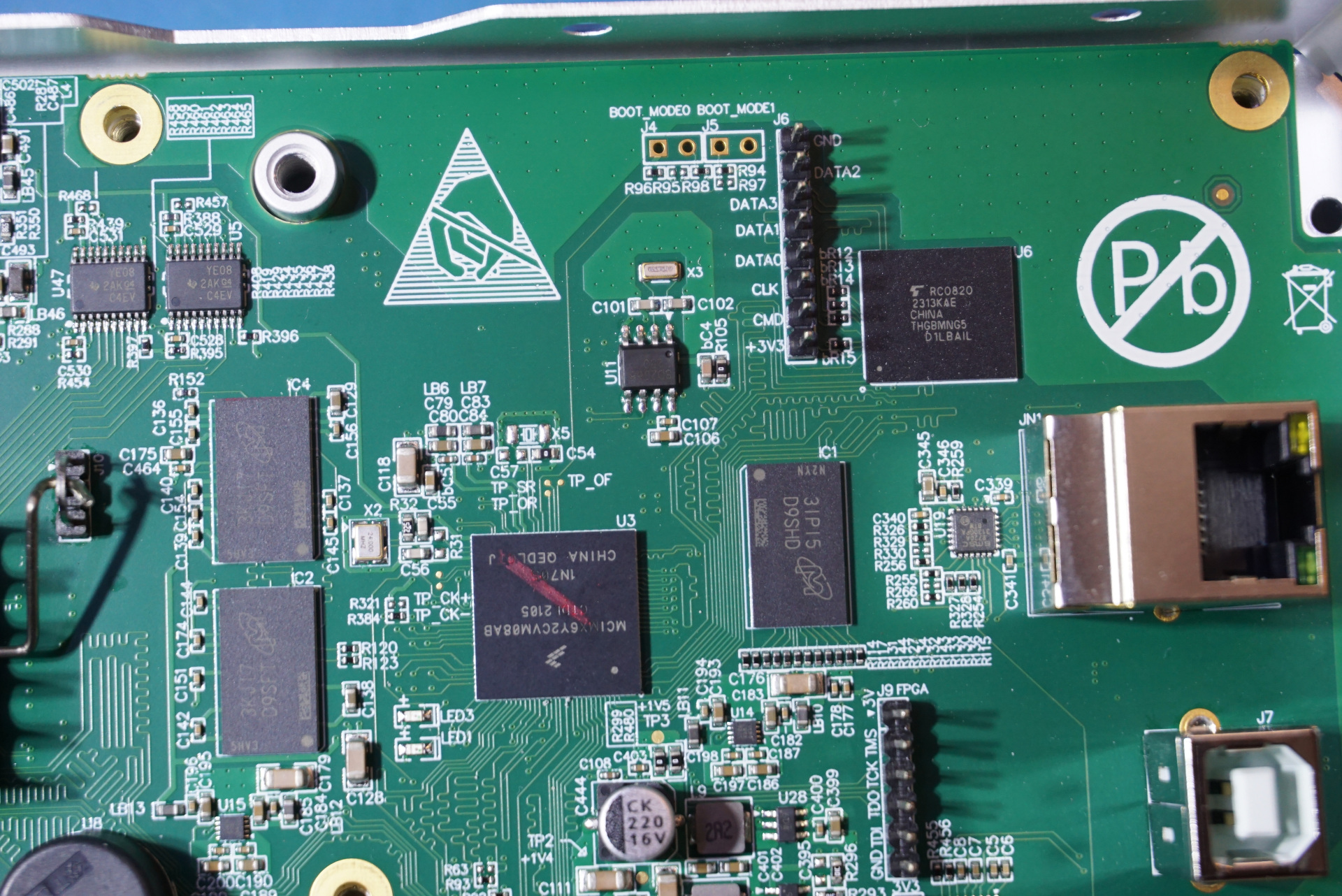
In the picture below, you can see the DDR memory chips. The application processor is a MCIMX6Y2CVM08AB which features an Arm Cortex-A7 core. The ethernet transceiver used is an SMSC 8720A, which is located next to the ethernet port. I am not entirely sure what that chip with the RC0820 marking is.
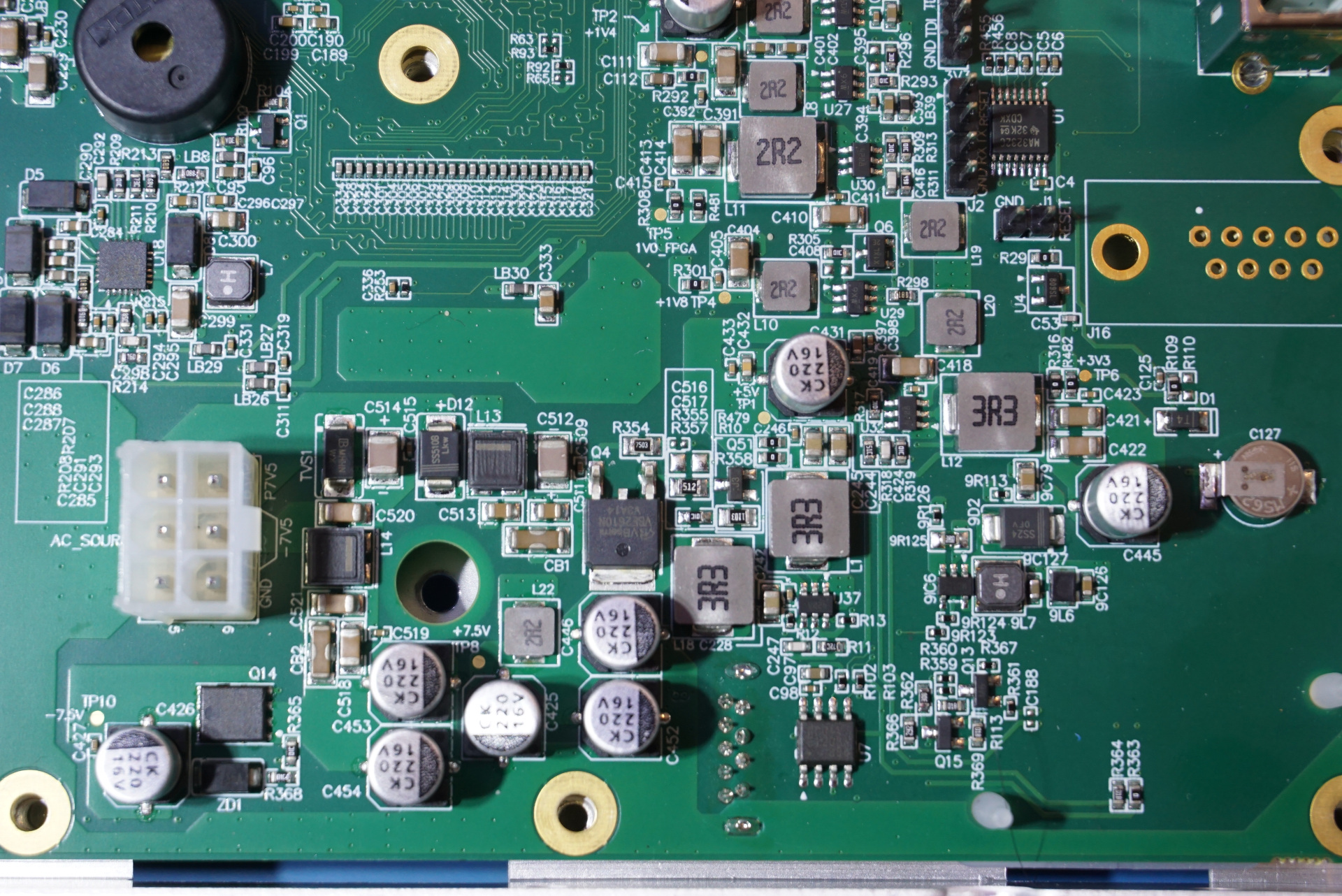
Here are some additional pictures.
Teardown video:

