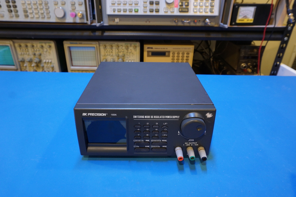
I recently picked up a BK Precision 1696 programmable switching power supply off eBay. Unlike many of the vintage test equipment I did teardowns with in the past, this model is still in production today. The one I got was sold with a damaged LCD screen and thus I paid very little for it. Of course, a brand new one would cost around $300.
My original plan was to find a replacement LCD and restore the unit to its original full functionality. But the LCD used in this unit is likely specifically made for the 169X series of power supplies and through some initial research I realized it would be extremely difficult to get hold of unless I could find a donor unit with a functional LCD inside. After I received the power supply, I realized that it had more issues than just the broken LCD itself. During my initial testing, I found that the output would not reach higher than 10 to 11 volts even with the over voltage protection set to the maximum value (20.5V). So clearly I have more homework to do, and for the time being let’s simply strip it down and see what’s inside.
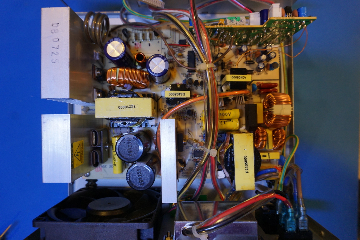
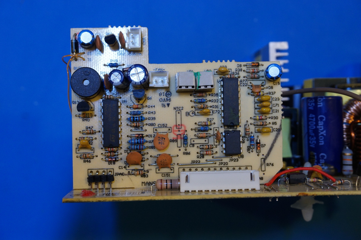
Upon opening the case, you can see the main switching power supply board, the digital controls are located on a separate front panel board. From a first glance, I was somewhat disappointed to see the quality of the construction inside. Besides the subpar PCB material used, you can also see quite a few bodged wires and seemingly out-of-place component placement. Keep in mind that what you are looking at is what supposed to be a piece of expensive professional test equipment.
|
|
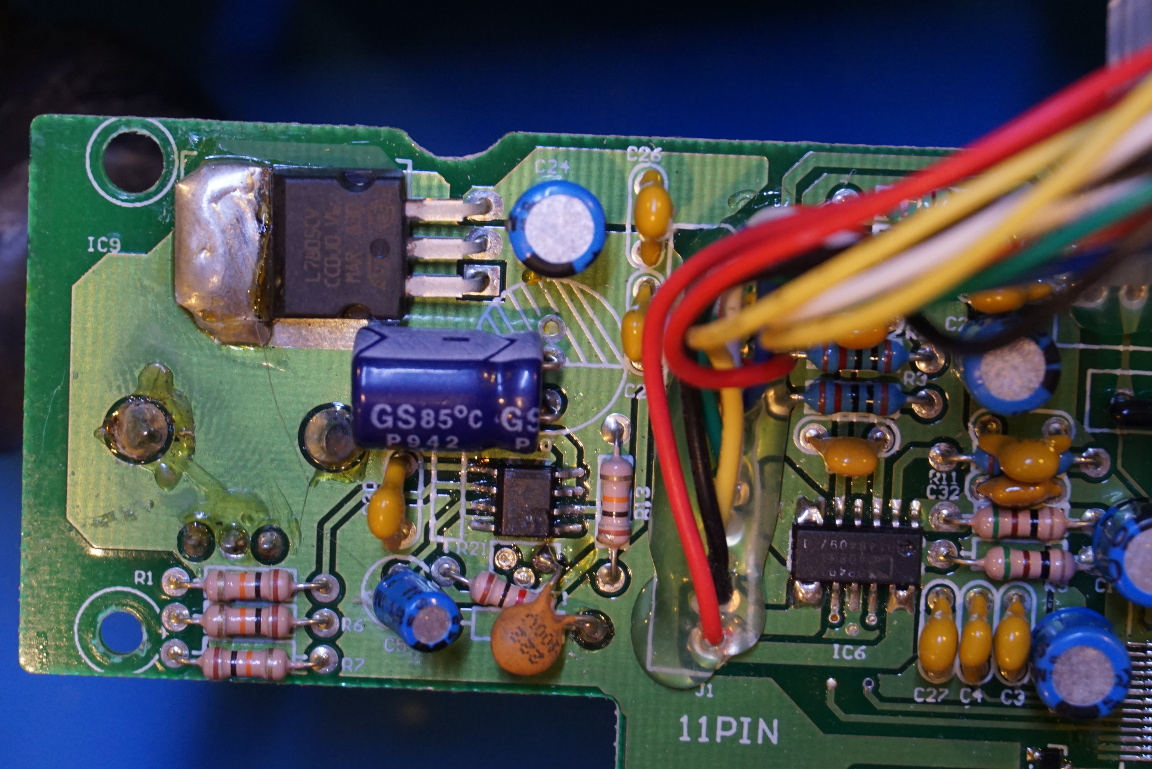
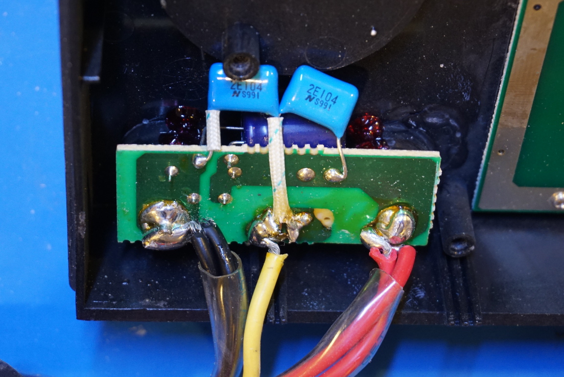
Here are just a few pictures to prove the point. To the left below is the corner of the front panel processor board, take a look at the flux residue and the glob of solder on the regulator heatsink! Signal wires are simply just hot-glued in place instead of using connectors. And the image to the right below is the output terminal board on the front panel. It almost looks like that the soldering iron was not powerful enough for the job. Although it could be true that someone had serviced this unit before but given the widespread issue we can see inside this unit, there is little doubt that the construction quality is subpar.
|
|
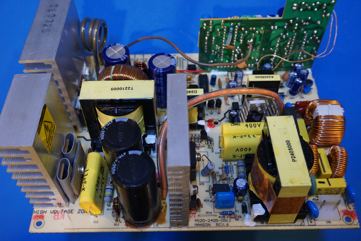
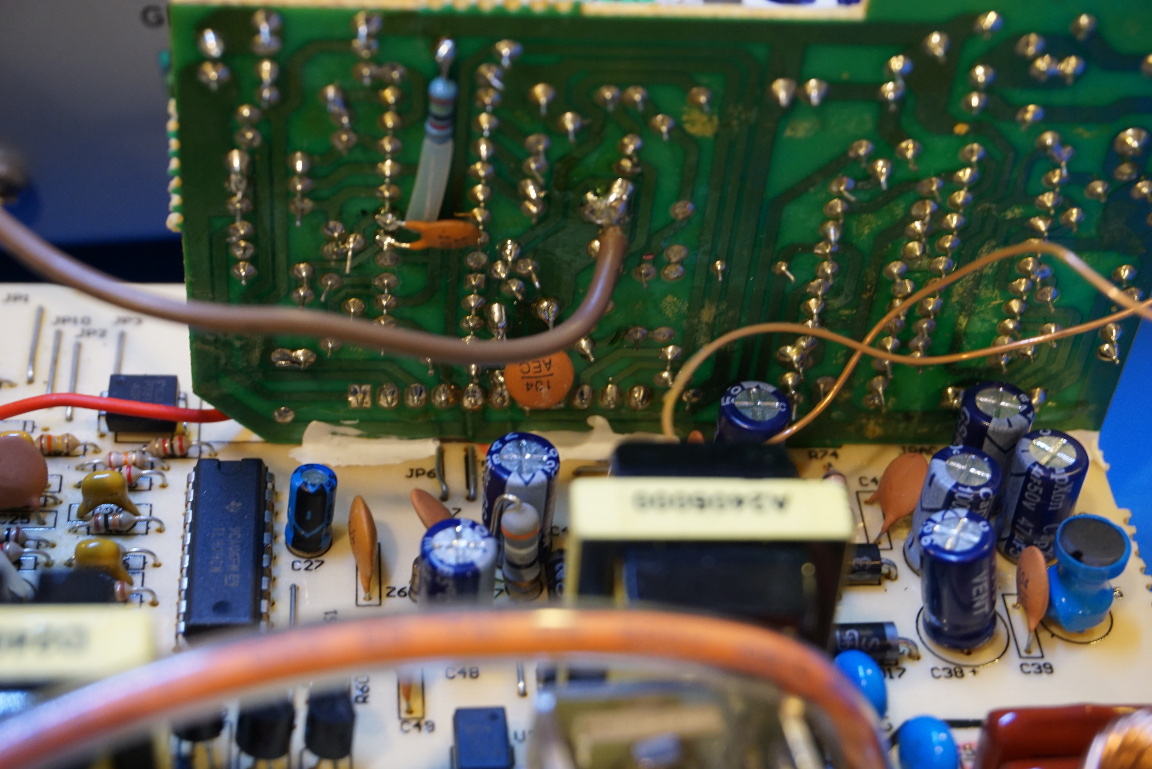
And the bodging continues. Here are just a couple more pictures to illustrate. In the picture to the left below, you can see bodged components on the backside of the riser board and the two thin wires from the transformer are actually connected to the riser board directly. A wire tapping into the current shunt was simply connected in a point-to-point fashion: from the back of the riser board to the current shunt resistor coil directly. Who needs a separate solder pad for that?
|
|
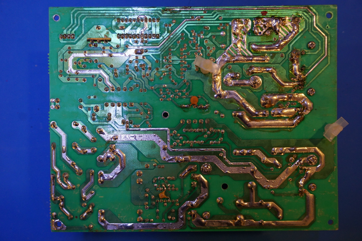
As if these were not bad enough, take a look at the soldering job on the main PSU PCB below. While it could be the case that someone repaired the unit before, the prolific signs of poor soldering is evident that many of the components were simply soldered willy-nilly without too much thought about quality. I would certainly hope that the problems I am seeing here are just one-offs as for a brand name such as BK Precision this kind of workmanship is unacceptable.
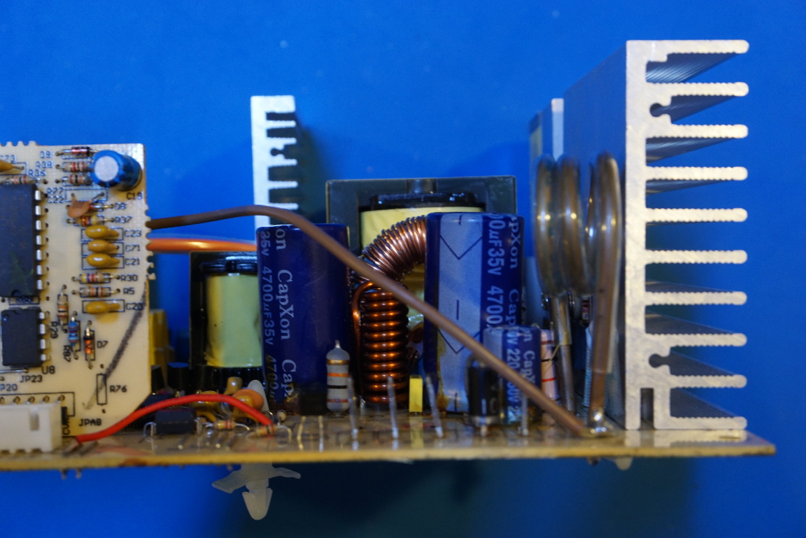
Construction quality aside, let’s take a look at this programmable switching power supply in a bit more details. On the main board you can spot an MC33262 power factor controller. And the main PWM controller chip is a TL494 which I happened to have touched upon in one of my previous posts. The riser board has two general purpose LM324 opamp’s and an OP27G low noise precision opamp. Judging from the signal connections on the board I think it is for over-voltage/over-current detection as well as for the fan temperature control.
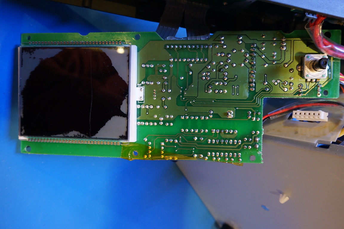
The picture below is the board mounted on the front panel. It houses the digital control logic. Towards the bottom you can see that signals are outputted to an RS-485 port and an RS-232 port via opto-isolators. The controller chips used are MAX485 for the RS-485 and MAX202CPE for the RS-232. An eight channel analog multiplexer/demultiplexer chip CD4052BC is also used here.
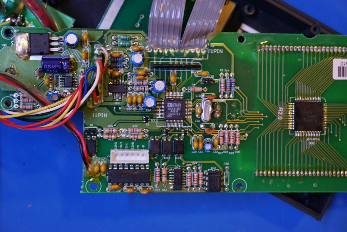
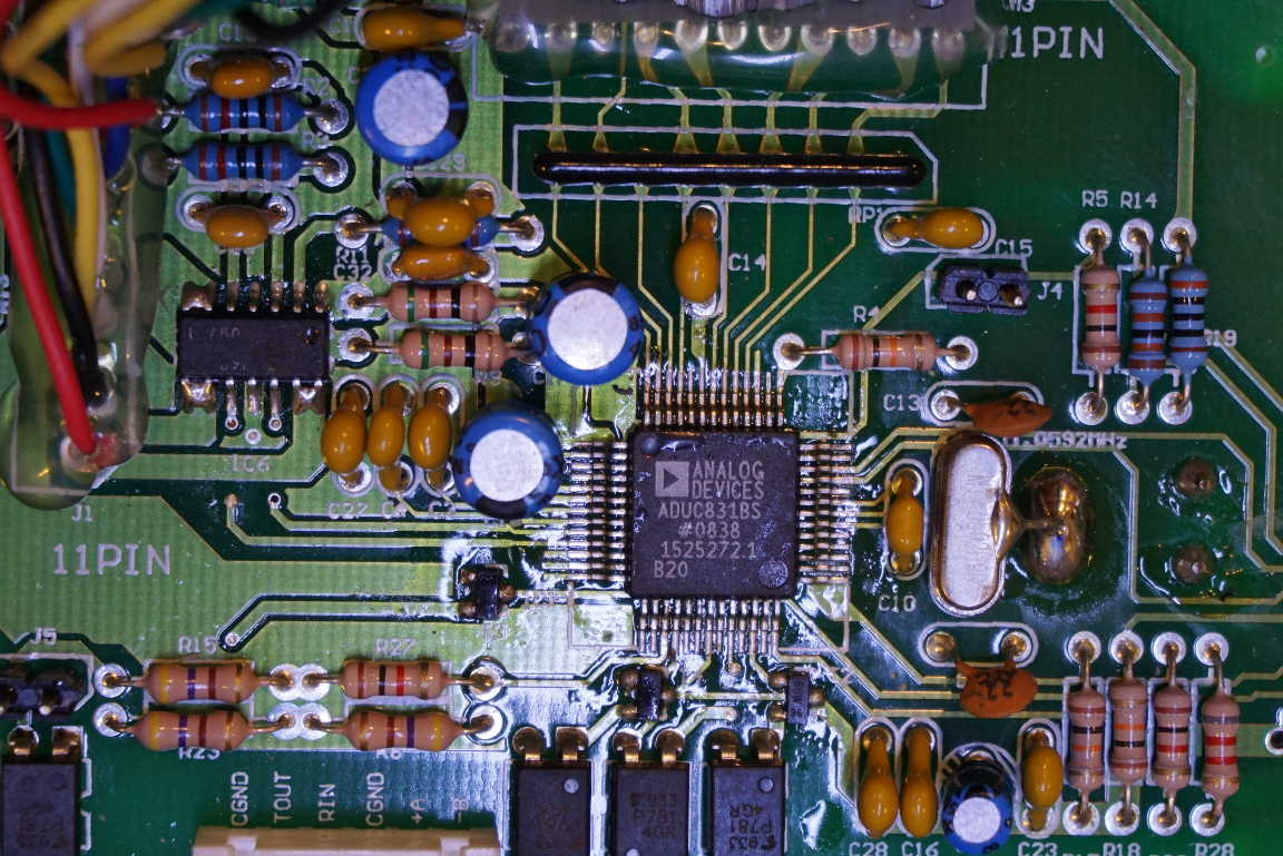
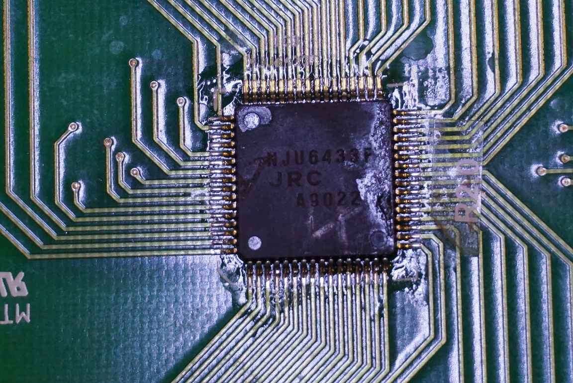
The microcontroller used in this programmable power supply is an ADuC831BS. It is actually a very potent 8051 chip with multiple 12-bit ADC’s and DAC’s. And the LCD driver used is a NJU6433F, which uses I2C protocol and drives the individual segments on the LCD. (Correction, it is not I2C, but rather a serial protocol that is similar to SPI).
|
|
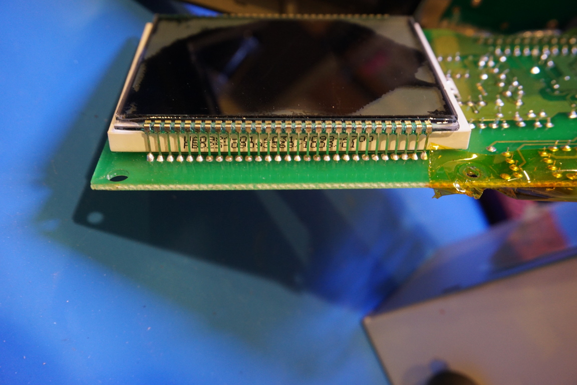
And here are a couple of pictures of the broken LCD itself. The LCD has 56 pins and looks to be a custom part. Without a replacement LCD, I would need to tap into the I2C bus and decode the signals so I can use some custom circuitry to drive my own LCD for displaying information. At least that is a possibility.
|
|
So my plan is to first investigate why the output voltage could not be adjusted higher than half of the rated output and then look into reverse engineering the LCD communication.
Below is a video of this teardown:

