I bought a USB wall outlet adapter recently so that I can free up my wall outlets while charging my phones and tablets. Of course, before putting it into use, I wanted to open it up to take a peak inside to see if it was properly engineered and at least to make sure that it would not be a safety hazard at the least. After all, this USB adapter is meant to be plugged in all the time.
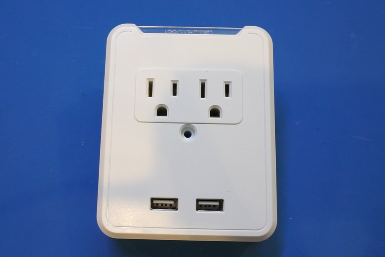
This USB charger/wall adapter is meant to be mounted on the standard vertical dual outlets, it even has a center hole to allow it to be mounted semi-permanently and more securely. Similar USB wall outlets are a dime a dozen, the one I bought is branded as “MVMT” and can be found in many US stores.
Specification wise, the adapter is rated to provide 2.1A for its USB output. I did some load testing with an electronic load I built before and it appeared that the 2.1A is rated for the combined output from both USB ports. You can see my testing in the video linked towards the end of this post. This means that if you are charging two devices using this adapter, charging time will be lengthened as the 2.1A output current has to be shared between the two channels.
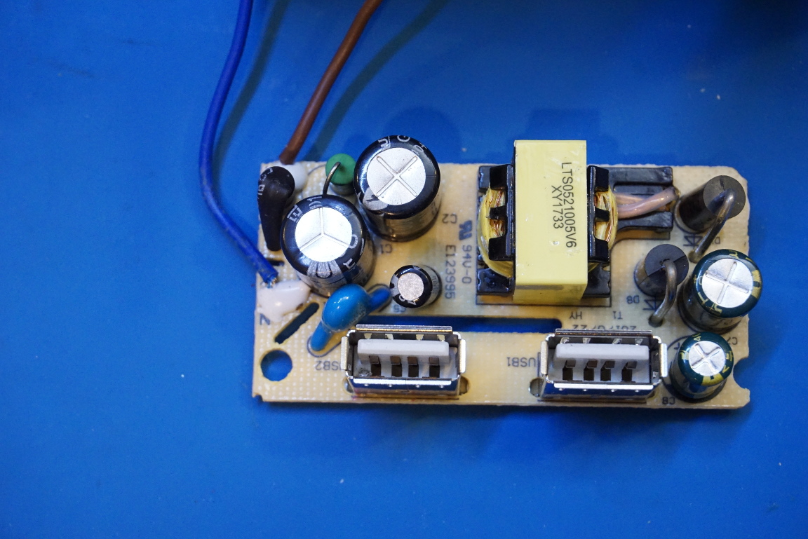
The internal build quality of this MVMT USB adapter is actually quite good. Two PCBs are used in this adapter. One is for surge protection and the other one is for the switching power supply that generates the 5V output rails.
If you look at the picture below closely you will see that the surge protection PCB has footprints for three MOVs, but only one is populated. This will no doubt limit its surge current rating. Perhaps a cost-cutting measure during manufacturing? There is also a blue LED powered by a capacitor dropper that illuminates an acrylic plate that has the word “PROTECTED” embossed on it.
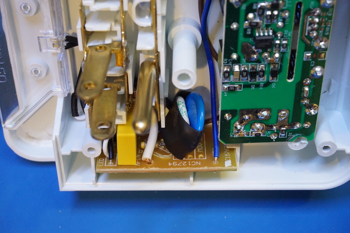
The power supply circuitry stays afloat in regarding to mains earth. But given that a fully isolated switching supply is used here and the apparent wide isolation and the inclusion of isolation slots at many high voltage locations, safety should not be a concern here.
The switching power supply is based on a single 8 pin chip. Unfortunately I couldn’t find any information base on the markings on this specific chip. Nevertheless, this kind of single chip design is rather common. OnSemi’s NCP1000 series for example falls into this category.
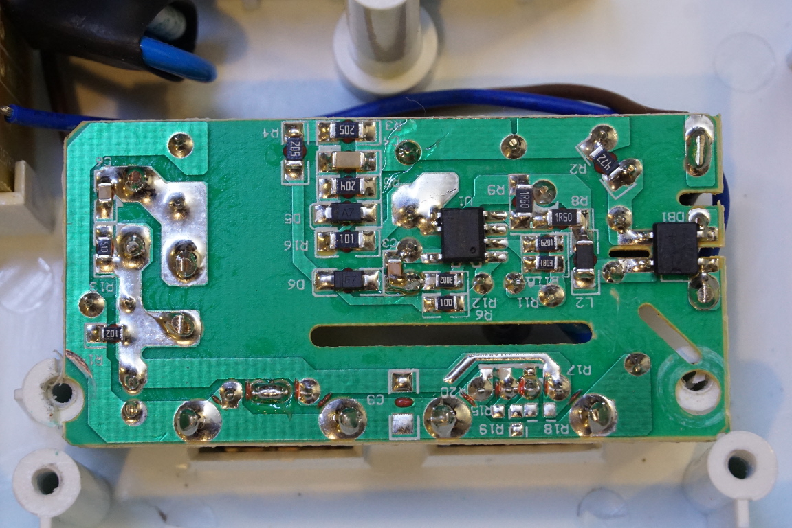
There’s not too much going on on the other side of the main PCB. Take a look at how far the output from the switching transformer extends. This arrangement is to ensure maximum isolation distance between the primary and the secondary.
In the video below, I did some performance testing followed by a teardown:

