In this blog post, we will take a look at a Waveform 600 MHz to 6 GHz ultra-wide-band (UWB) cross-polarized 4×4 MIMO panel antenna. It is designed for cellular 4G LTE / 5G hotspots and routers.
According to the datasheet, this antenna operates in the following four frequency bands: 600 – 698 MHz, 698 – 960 MHz, 1710 – 2700 MHz and 3300 – 6000 MHz with gains ranging between 4 dBi to 8 dBi depending on the operating frequency bands. This frequency range pretty much covers the entire cellular frequency band used for 3G and 4G LTE in North America. It also covers the low-band (600 – 850 MHz) and mid-band (2.5 – 3.7 GHz) 5G cellular spectrum. When using with wireless routers, it can support both the 2.4 GHz band and the 5 GHz band simultaneously.
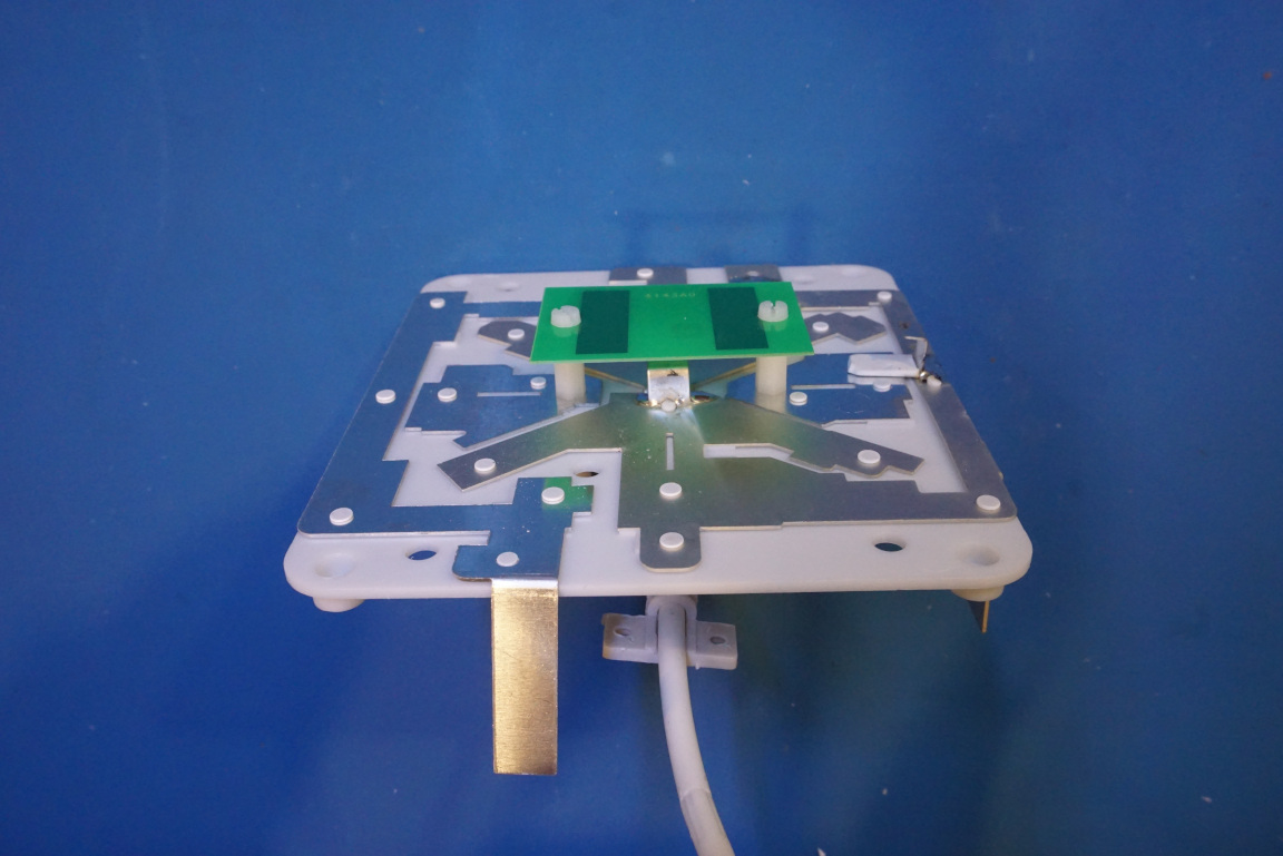
As I explained in one of the earlier teardowns, MIMO antennas essentially use multiple antennas to increase signal diversity. Once the antenna dome is removed, you can see four mostly identical antenna elements in two different orientations. With this design, each antenna element covers the entire 600 MHz to 6 GHz frequency range. This design approach is very different than what we saw in the teardown of a dual band cellular band MIMO antenna last time. In that antenna design, it essentially consists of two sets of cross polarized dipoles antennas with one set for each frequency band and a diplexer that is used to multiplex the two frequency contents.
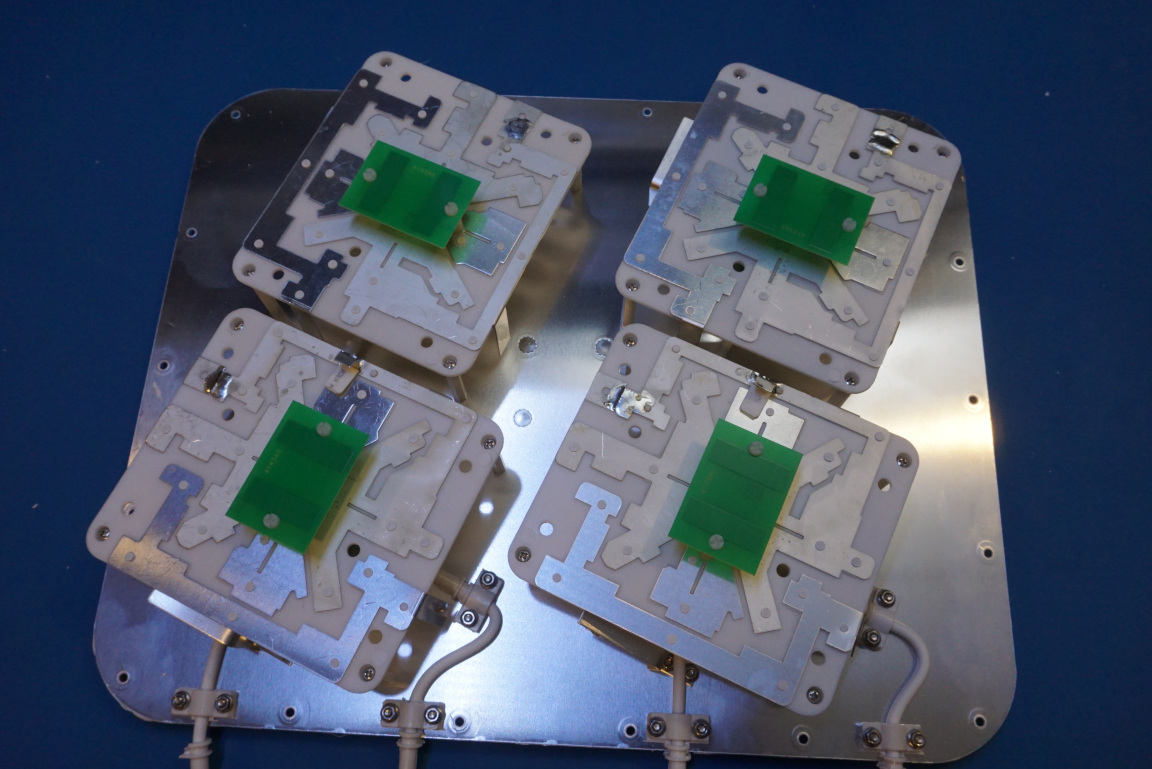
Looking at the arrangement of these antennas, you can clearly see that the upper two elements are rotated by 90 degrees compared to the lower two antennas. The green PCBs sitting on top of each antennas are dummy elements (there is a similar dummy element underneath of each antenna element as well). The orientation of the parallel traces align with the induced electric field. Thus within each side the two antennas at the top and bottom are orthogonally polarized (a.k.a cross polarized).
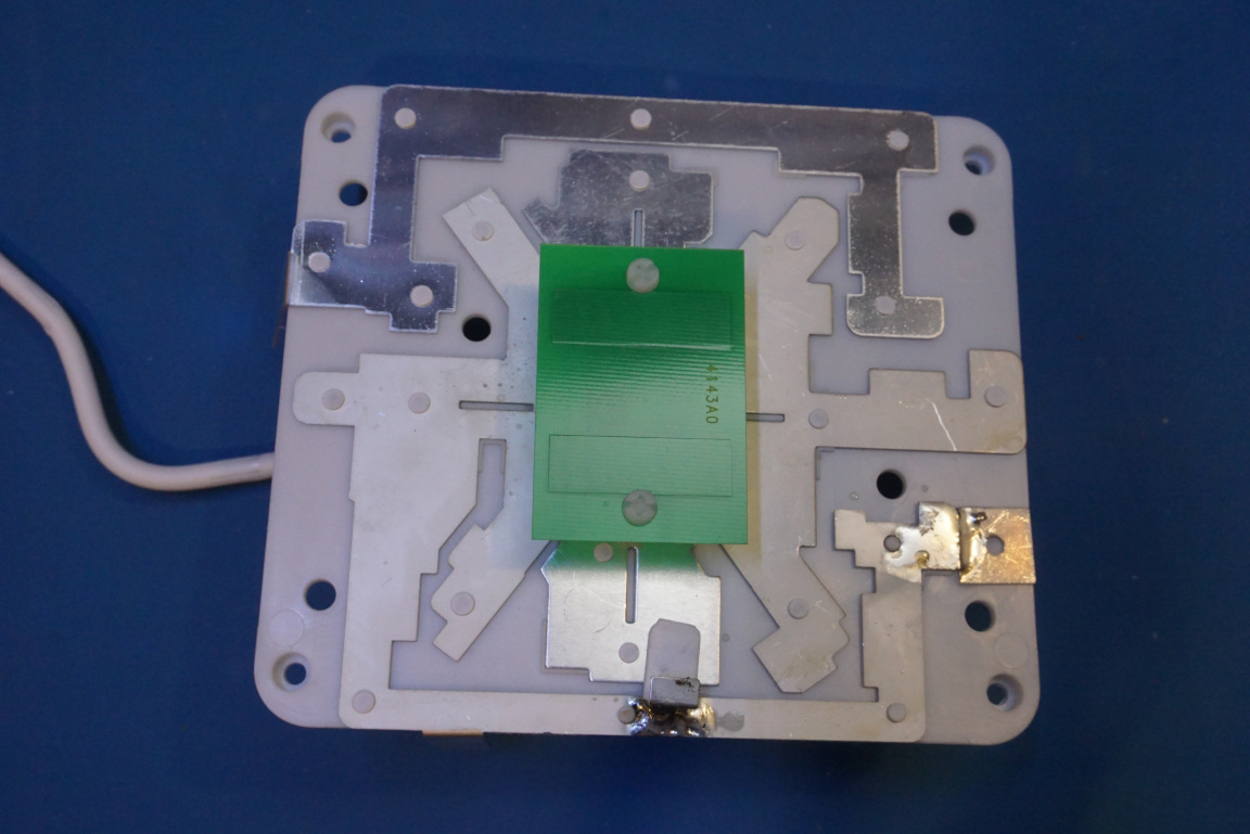
By removing one of the antenna elements, you can see it more clearly. This element is the bottom right one in the picture above. The picture to the right below shows the antenna element with the top dummy element removed.
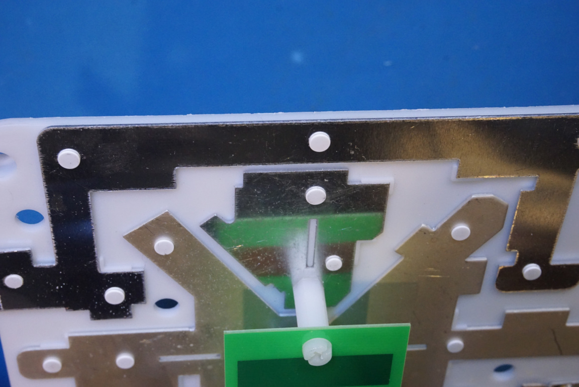
Here are a couple more pictures of the antenna from different angles. In the picture to the right below, you can see additional dummy elements. One common technique for increasing antenna bandwidth is by introducing some parasitic elements or dummy elements on the same plane of the driven element. The general idea is that if the resonant frequencies of these parasitic elements are slight different than the driven element, the overall frequency response is the superposition of the frequency responses of all these elements. Another technique is to increase the aperture of the driven elements.
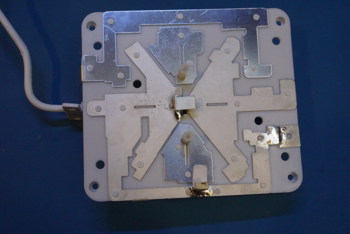
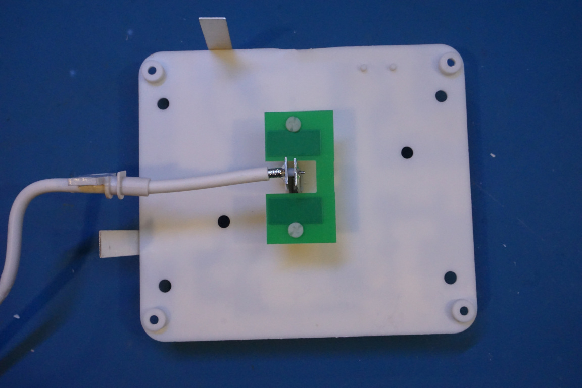
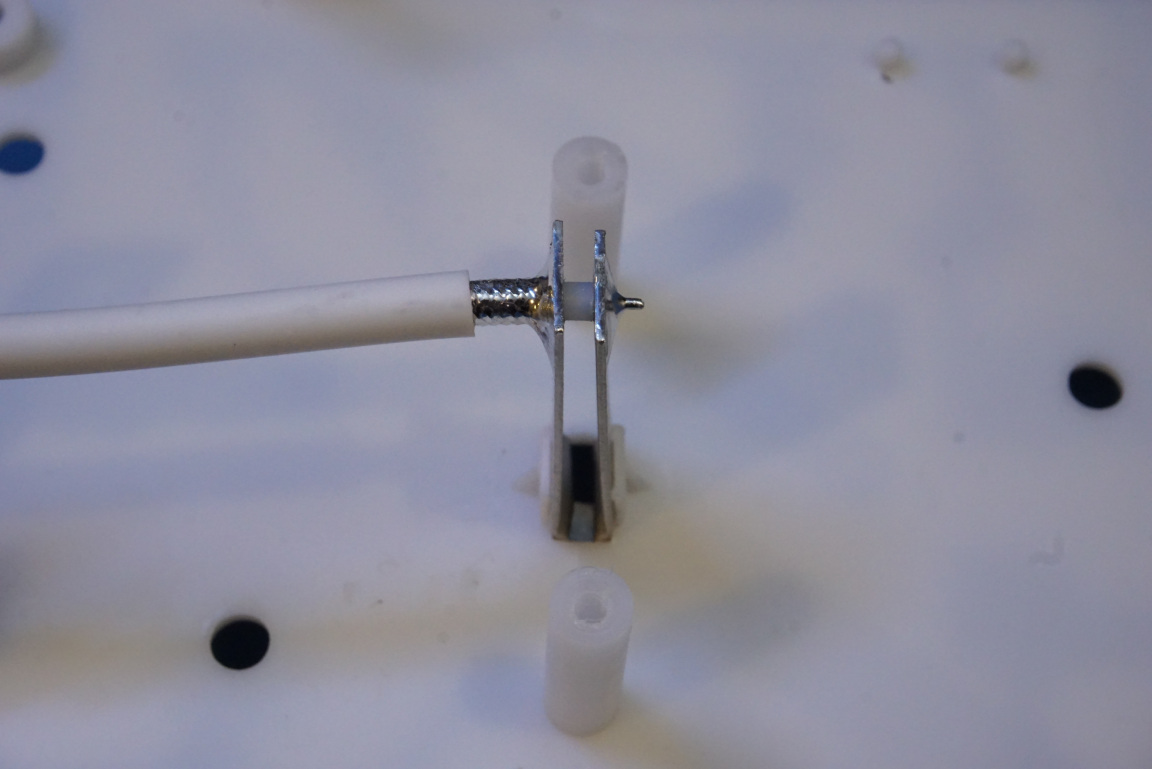
Here are a couple of pictures showing the underside of the antenna elements. In the picture to the right below, I removed the dummy element. You can clearly see how the coax feeds into the antenna. Note that unlike many antenna designs, the ground plane is not connected to the chassis back plane. In fact the grounds of the four antenna elements are not physically connected.
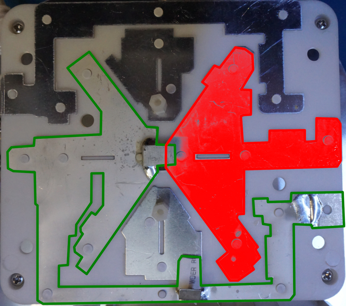
In the picture below, you can see the driven element (connected to the coax center conductor) marked in red. The shape marked in green is connected to the coax’s outer shielding. The three pieces that are not outlined are the dummy elements. The internal slots are also used to increase the bandwidth. Typically, the shape of these elements are carefully designed with commercial high frequency simulation software (HFSS) using finite element analysis.
Note that the ground plane wraps around the driven element. This changes the antenna radiation pattern and thus allow minimum interference between the two adjacent antenna elements with the same orientations. This is some times referred to as pattern diversity in MIMO antenna designs which is commonly used for reducing mutual coupling and maximizing diversity gain.
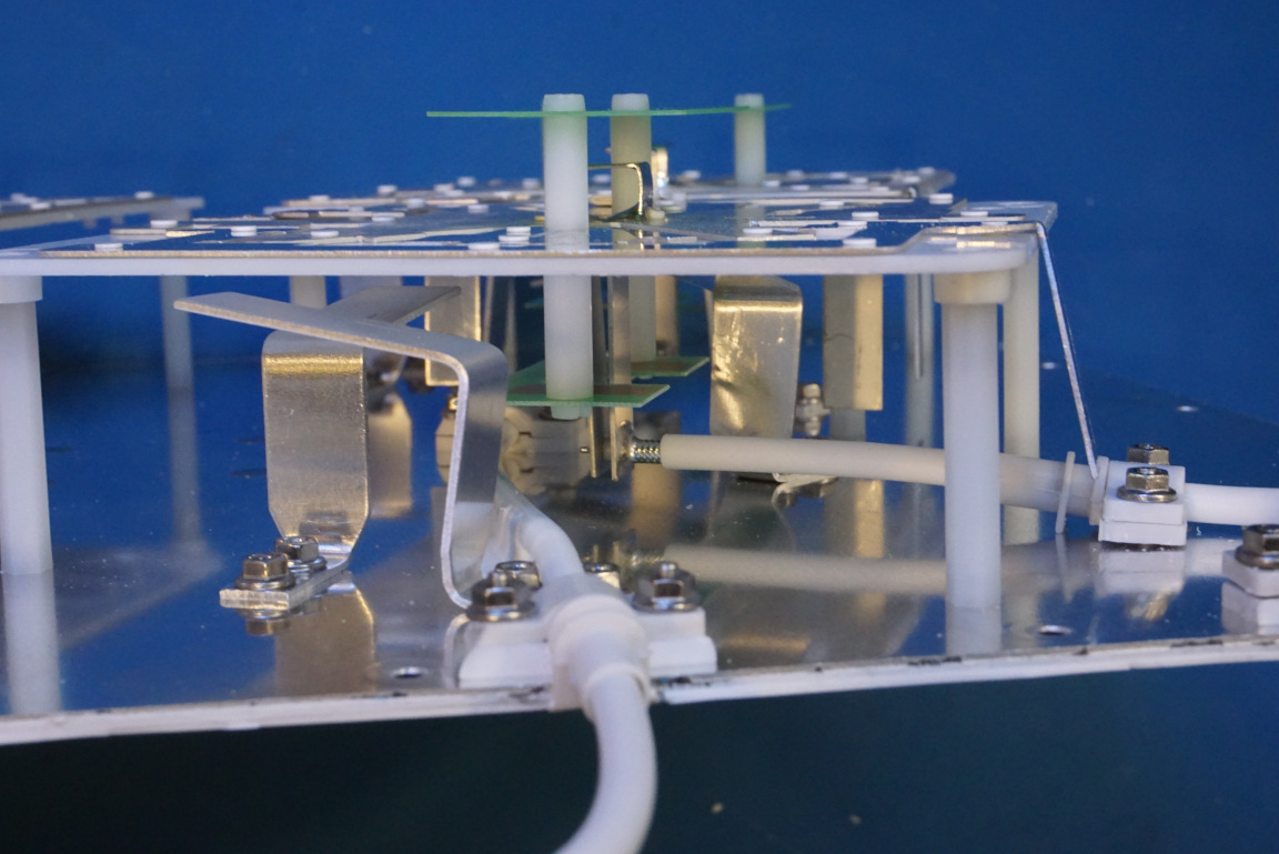
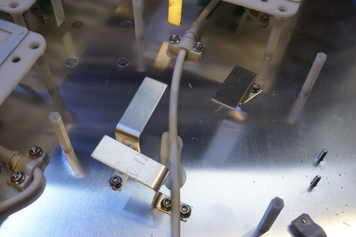
In the picture below, you can see three protruding metal stands on the back plane under each of the antenna element. I believe these stands are used for tuning the frequency response.
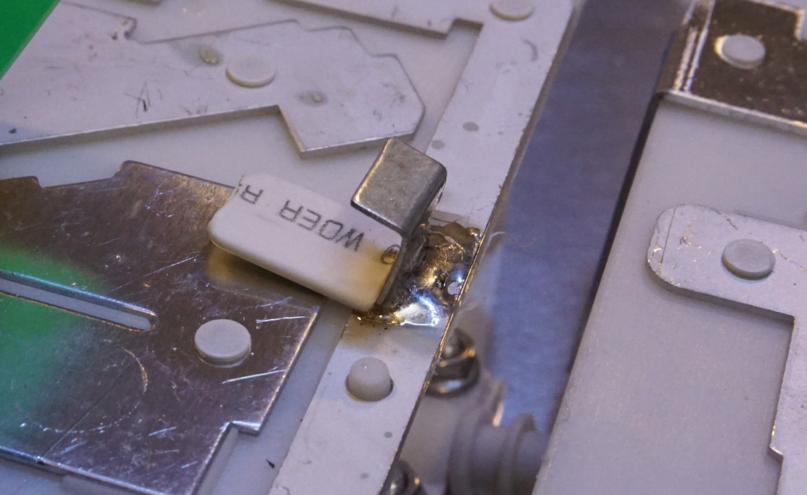
If you look at these antenna elements carefully, you will notice that the bottom two are slightly different than the top two in that they both have a metal tab soldered onto on side of the ground trace. Again, it is probably used to fine tune the frequency response or perhaps alter the radiation pattern to achieve maximum cross polarization isolation?
Below is a video of the teardown. In this video I also used a nanoVNA to verify the return loss (S11) and isolation (S21) between both the horizontal pair (with the same polarization) and the vertical pair (cross polarization).

