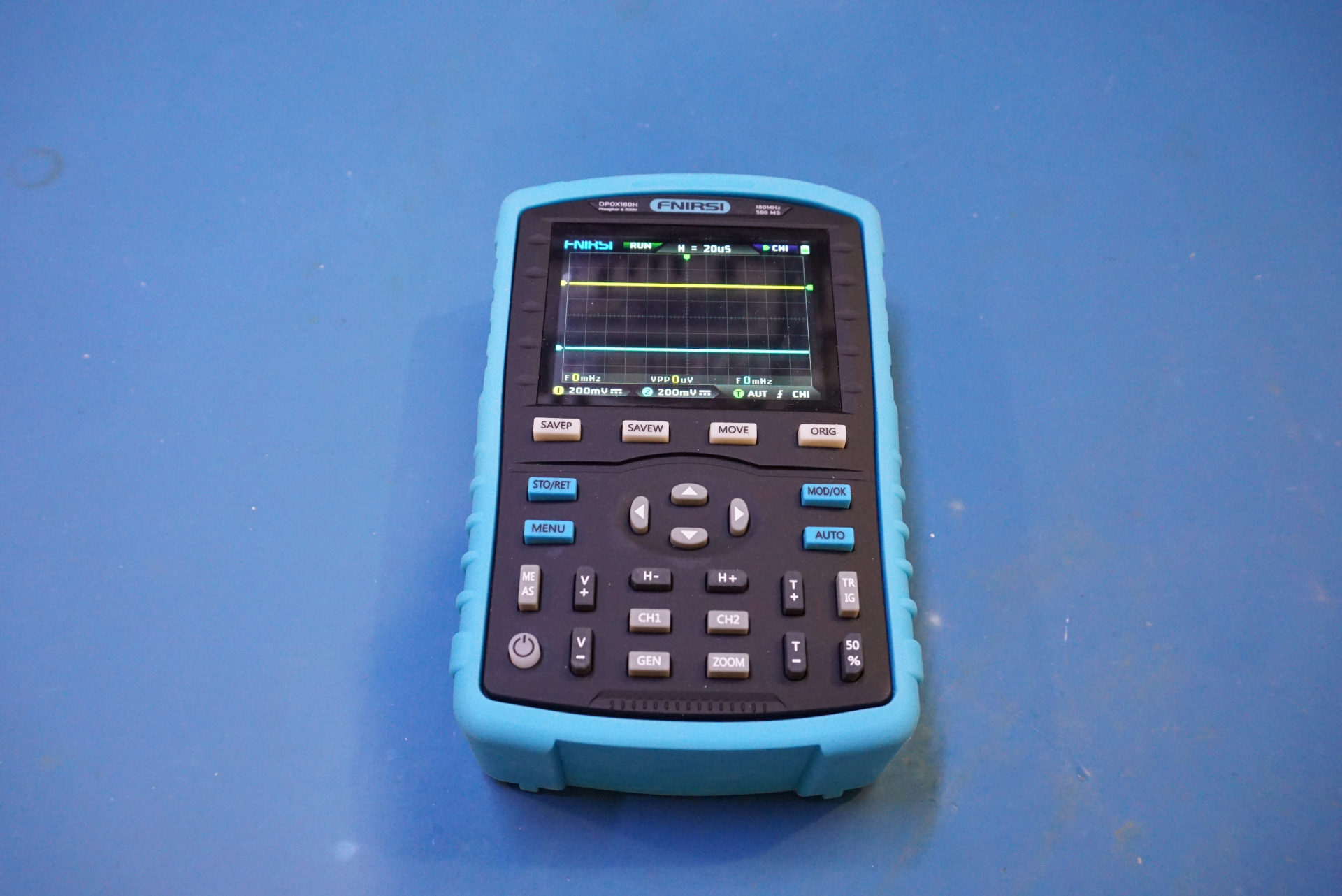
The FNIRSI DPOX180H is a digital phosphor dual channel handheld oscilloscope with a builtin function generator. It boasts a single channel bandwidth of 180 MHz. I was at first very skeptical of its bandwidth claim, but upon further verification, the scope was actually able to meet its specified bandwidth. For a budget scope that is just over $100, I have to say I am pleasantly surprised. You can check out the review video towards the end, but in this blog post I am going to share some of the teardown pictures.
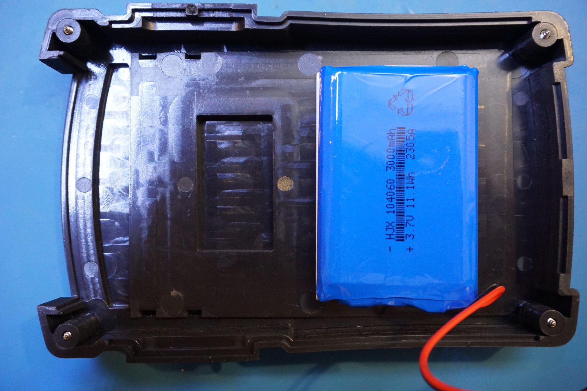
With the back cover removed, you can see the main circuit board with two large shielding cans for the two input channel front end circuitry. The battery is a 3 Ah one and offers plenty of runtime. I didn’t test the exact runtime but after working continuously with the scope for a couple of hours, the battery gauge barely dropped. So the included battery should be sufficient for extended use.
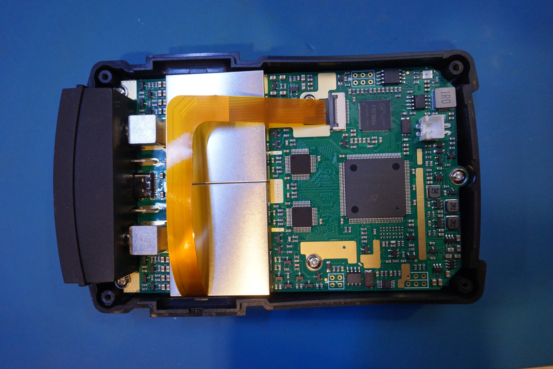
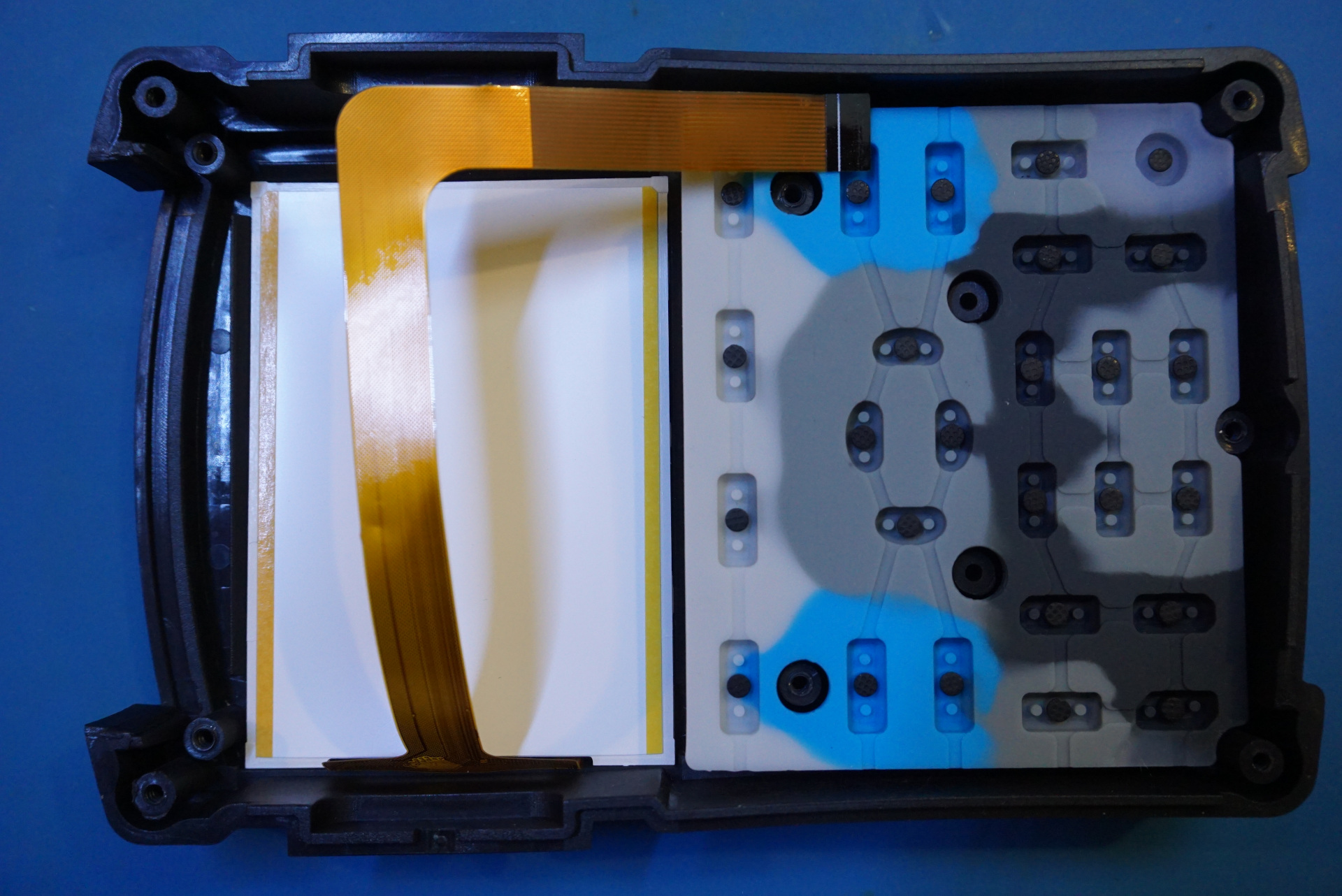
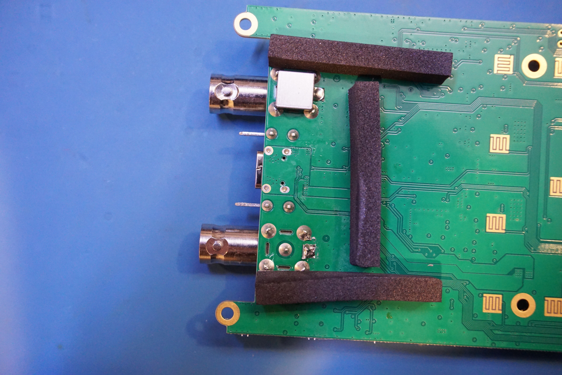
The LCD is mounted on the front panel and connected to the mainboard via a flat flex cable. This design is rather clean as it allows you to remove the main PCB easily. The picture to the right below shows the shielding can on the reverse side of the BNC input. Out of curiosity, I had removed one. I wanted to make sure there is no additional circuitry under this shielding can. As expected, this shielding is just for the BNC input and nothing else.
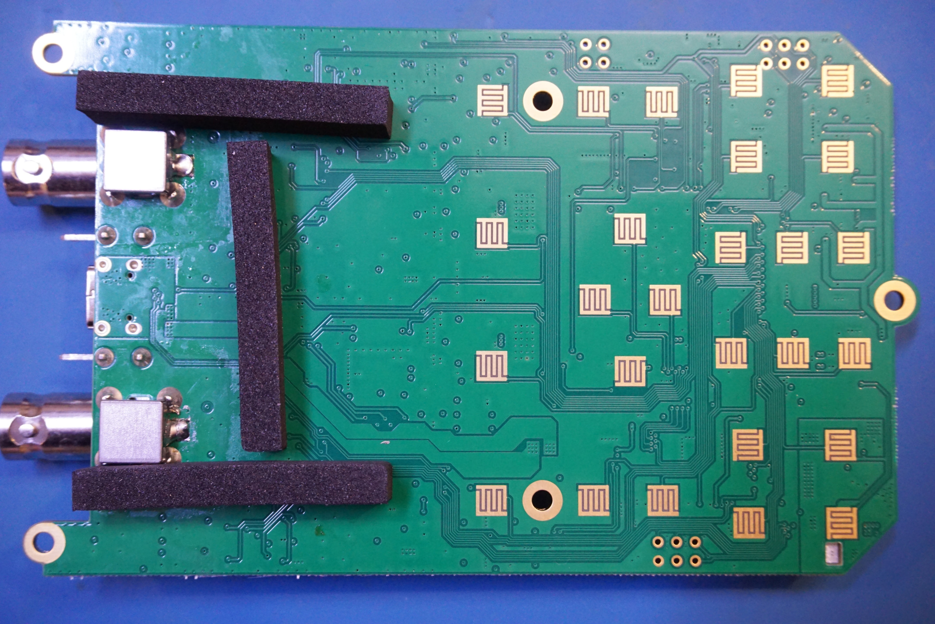
Here are a couple of pictures of the front side and back side of the main PCB.
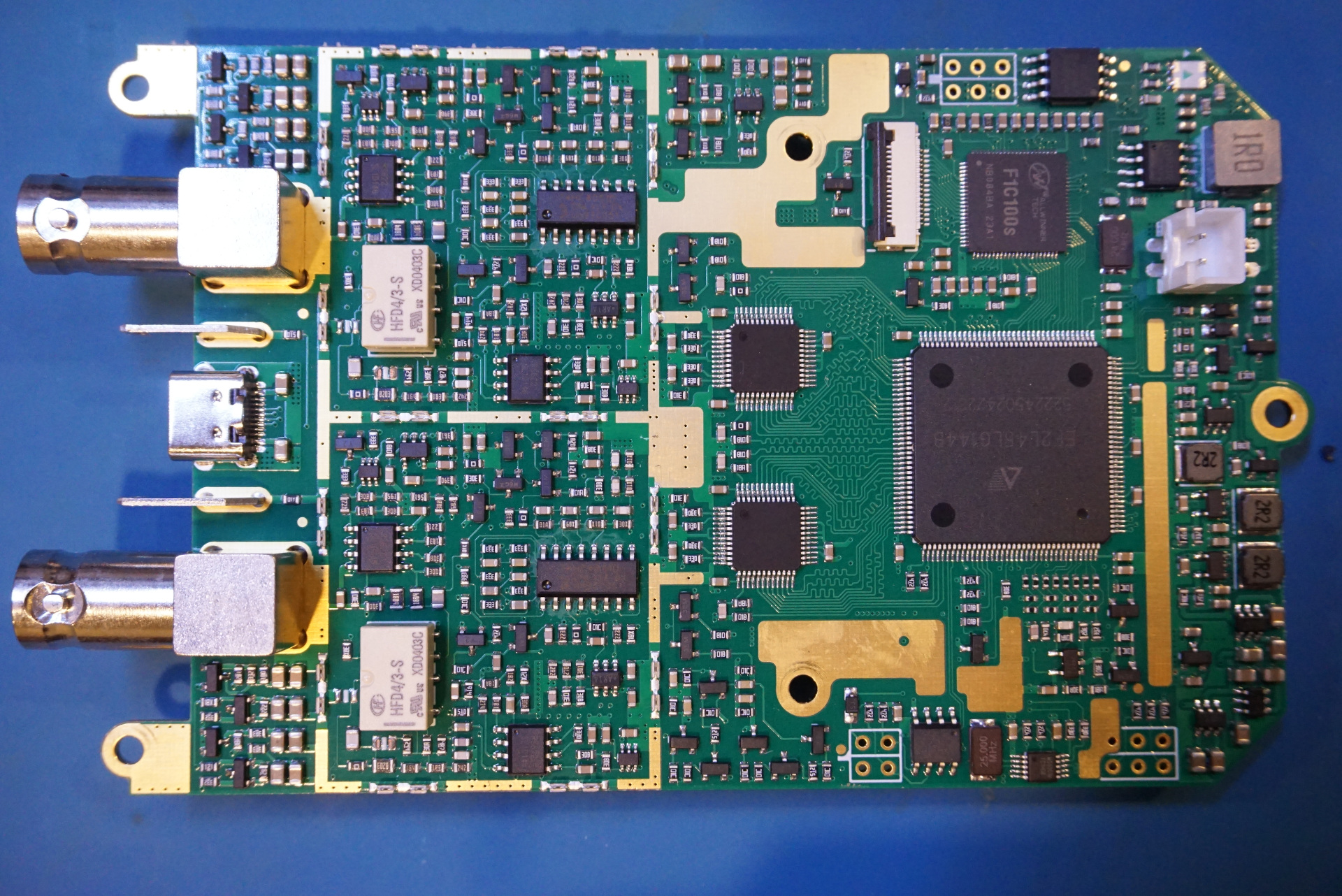
The front end circuitry does not have any adjustable capacitors which means you would not be able to fine tune the frequency response and the flatness of the front end. But keep in mind, this is a budget portable scope and this should not be an issue for its intended use. Plus there is no detailed specifications (e.g., gain accuracy, etc.) for the DPOX180H anyway.
From a casual glance, the front end amplifier is likely implemented with discrete transistors. There are a couple of 8 pin SOIC RS622 is a 7 MHz, rail-to-rail Opamps in each input sectio and there is a 74HC4051 multiplexer for each of the channels.
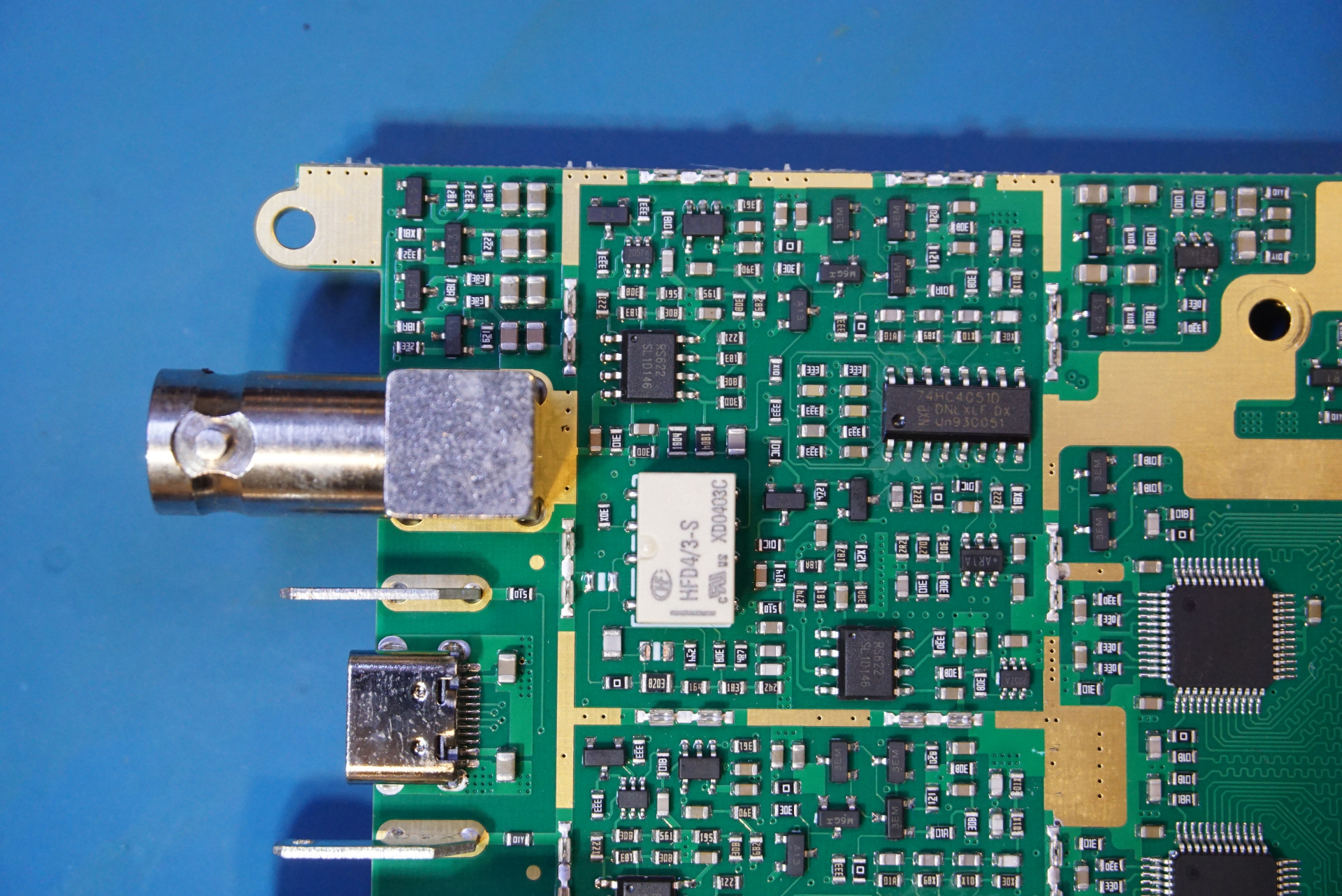
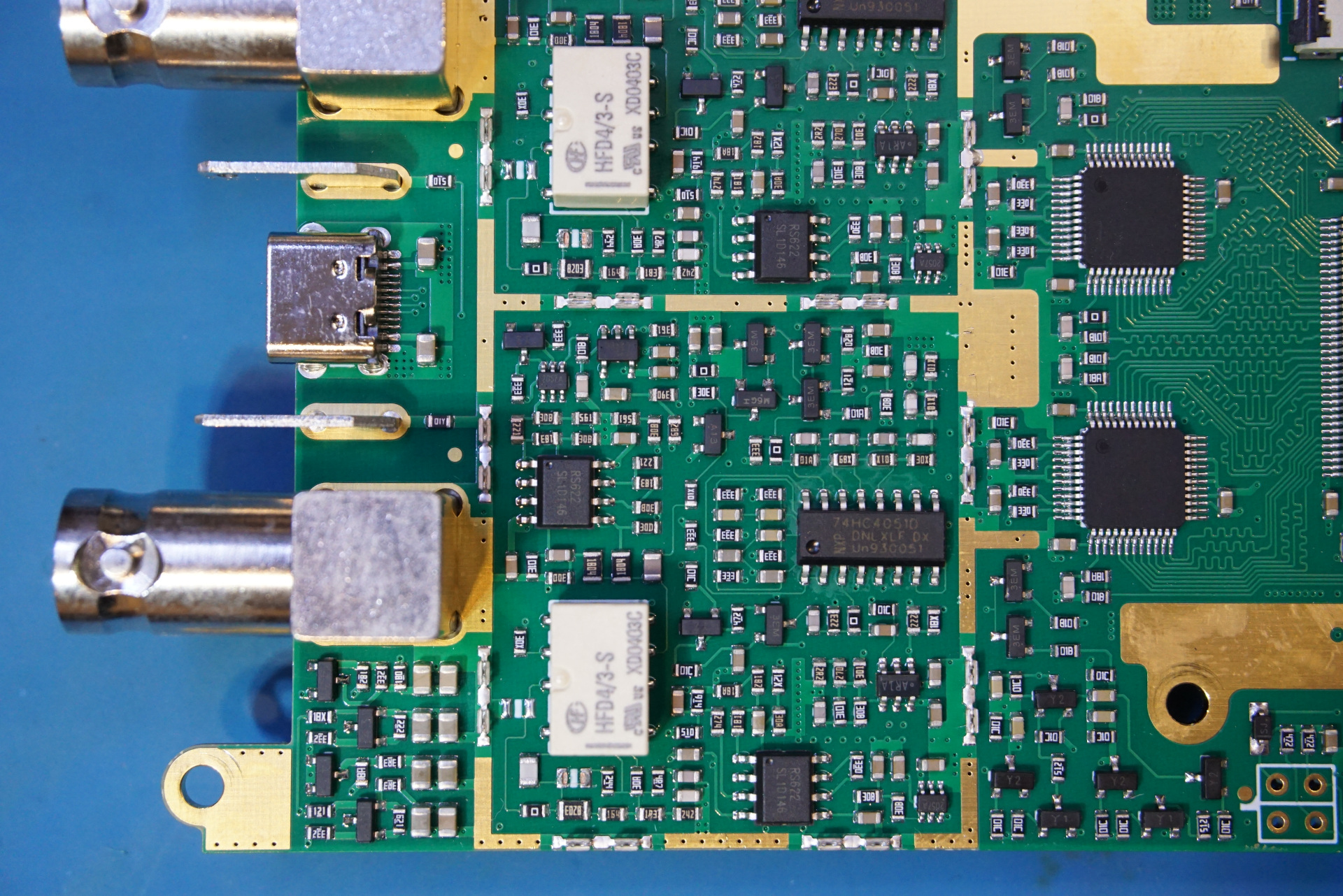
There are two ADCs used in this design. Although the markings on these ADCs have been erased, we can tell that they are using an interleaving sampling technique to double the effective sampling rate of the ADCs. So, each of the ADC is only running at 250 MSPS in this case. This design could allow manufacturers to use cheaper lower grade ADCs. As a drawback, the gain accuracy of each ADC and the clock stability would have significant impact on the interleaved sampling and we did see some acquisition stability issues during testing.
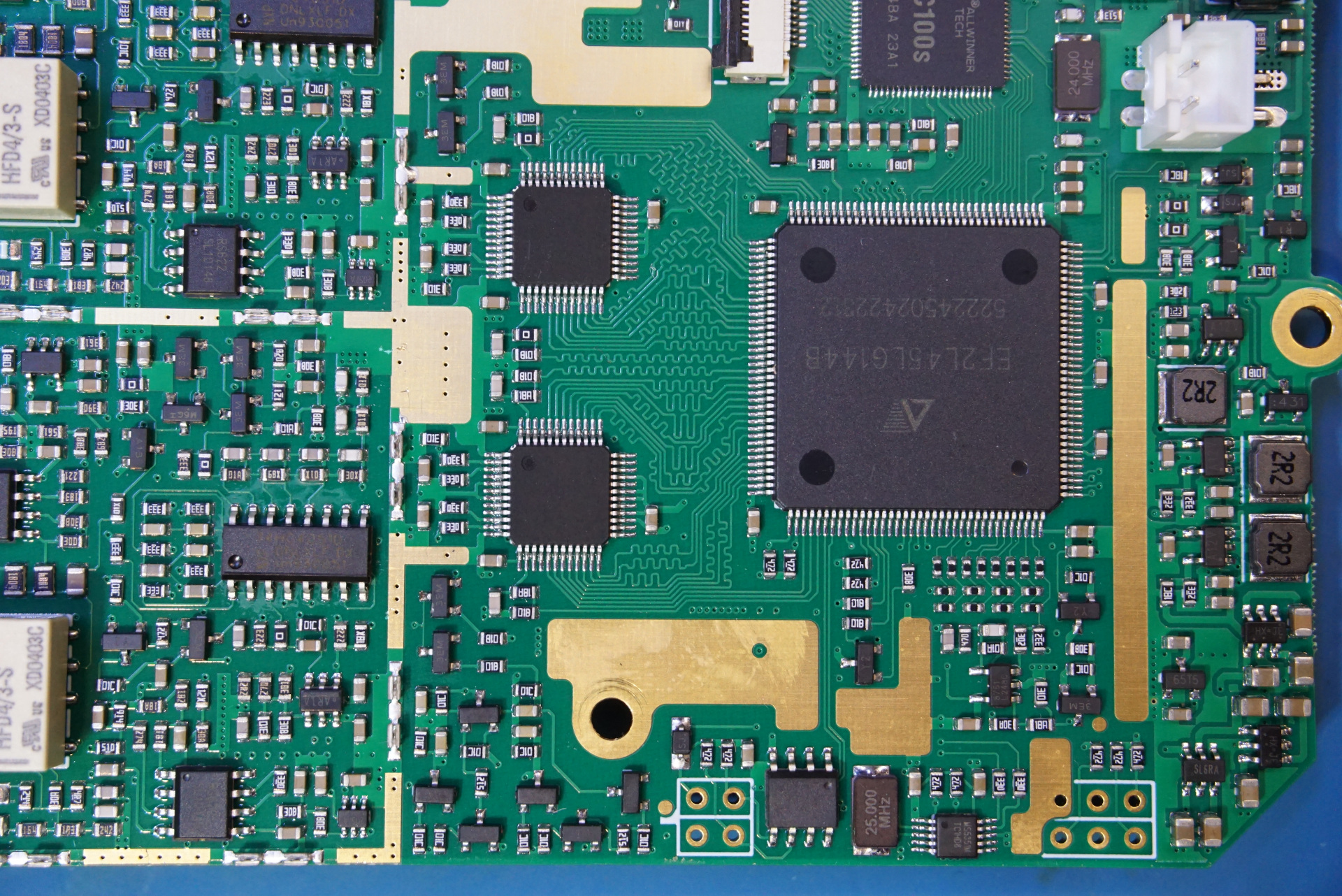
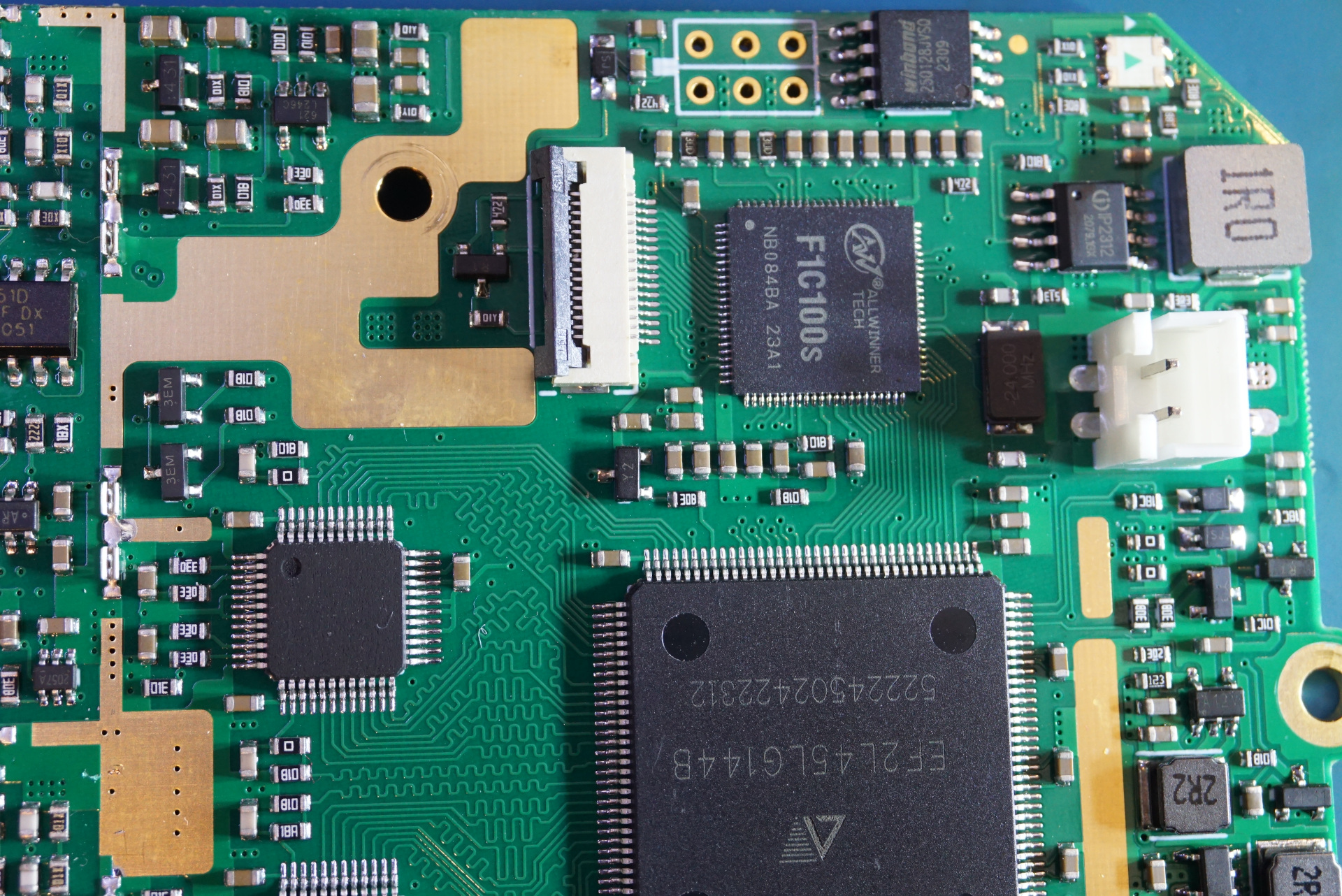
The main FPGA used is an EF2L45LG144B made by anlogic. And the application processor used is an F1C100s SoC wich contains an ARM CPU along with 32 MB onboard DDR memory.
You can also check out the review and teardown video of the FNIRSI DPOX180H below:

