I picked up an Amrel PPS-2322 programmable power supply from eBay recently. You probably have not heard of the Amrel brand before as American Reliance (Amrel) no longer makes power supplies nowadays. Its power supply division was acquired by AMETEK Programmable Power, a subdivision of AMETEK back in 2010. While Amrel power supplies had been discontinued, Amrel branded electronic loads are still being actively developed and sold by AMETEK.
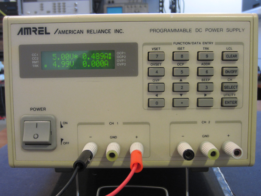
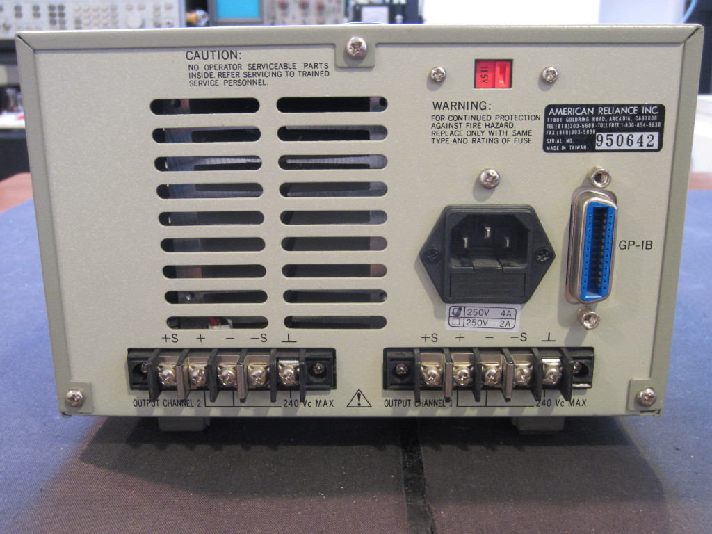
Amrel PPS-2322 is a dual 32V/2A programmable power supply. It has two fully independent channels. They can be used either separately in independent mode or used together in tracking mode. The power supply can be programmed via either the front panel keypad or via GPIB. Power supply outputs can be accessed via the front panel binding posts or the rear panel screw terminals. Note that the sense terminals are only present on the rear.
|
|
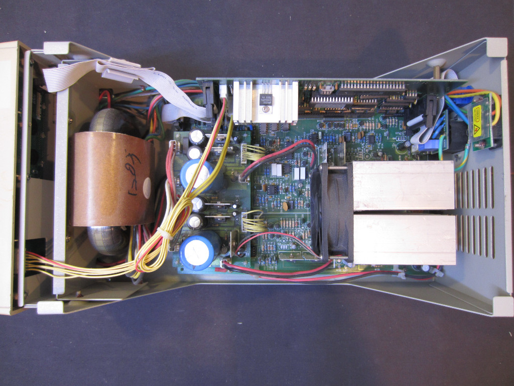
The top case cover is fastened by the three screws located at the back of the power supply. Unlike the typical test instrument case construction, this case does not slide off the unit. To remove the cover you will need to slide it back a little bit, pry the bottom of the case outward and then lift the case upward. After the top cover is removed, you will see that it was actually constructed to have a slightly narrower opening at the bottom so that the tension makes the cover a very snug fit.
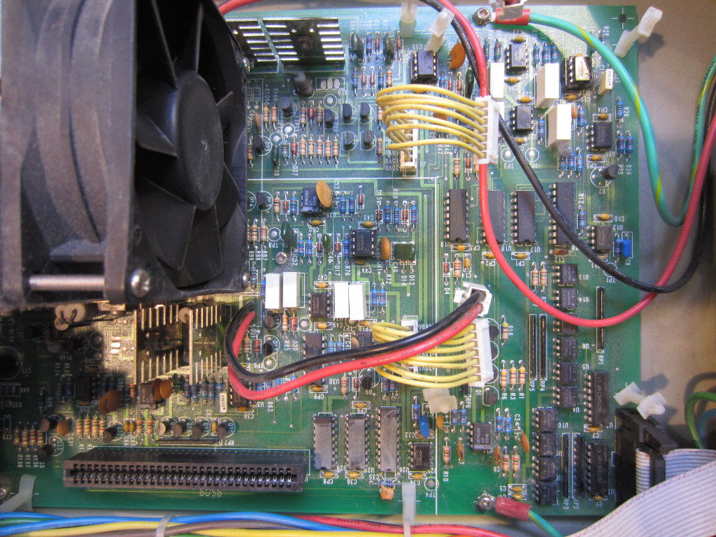
The picture below to the left shows the interior upon removing the case cover. As you can see the layout is rather clean. The main board at the bottom handles all the analog stuff and the plug-in processor board handles the programming and GPIB communication.
|
|
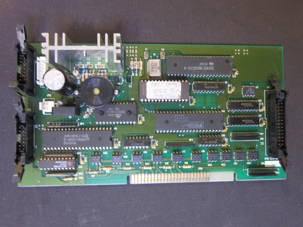
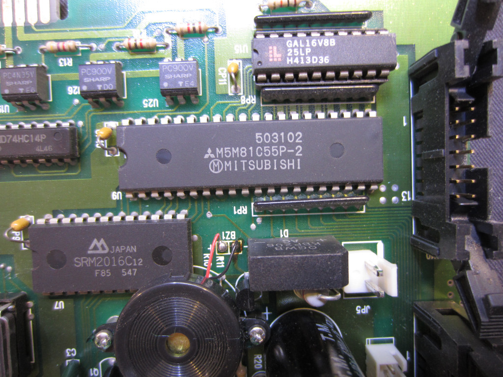
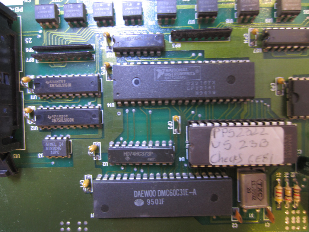
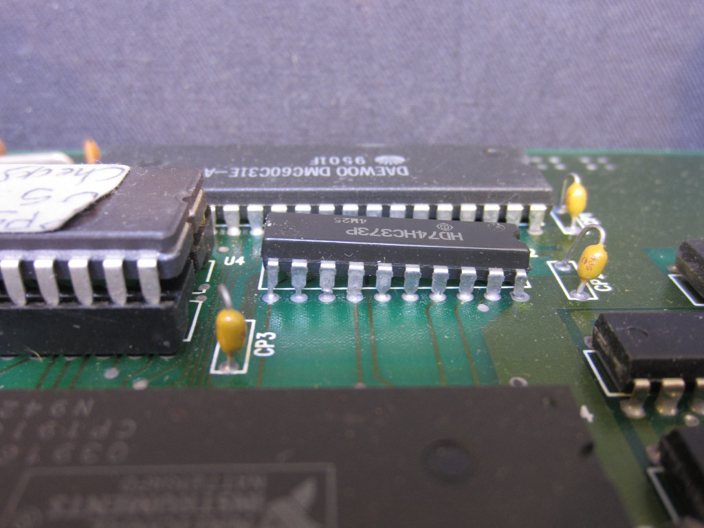
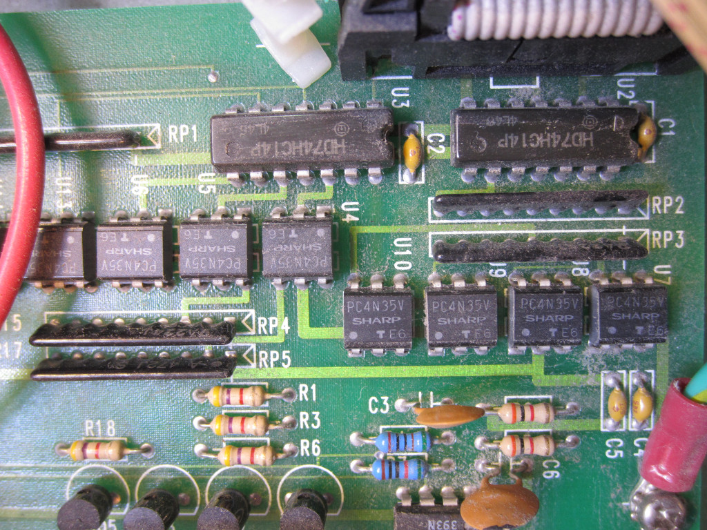
The processor board contains a CPLD (GAL16V8B) chip, two SRAM chips (MPM81C55P-2 is a 2K SRAM and SRM2016C is a 16K SRAM), and a 80C31 microprocessor (DMC60C31E-A, which is essentially a ROM-less 8051). The NI chip (CP19161) is presumably the GPIB controller (although I could not find any information on this chip). The firmware is stored in the UV-erasable EPROM (the firmware version of my unit is 5.23B).
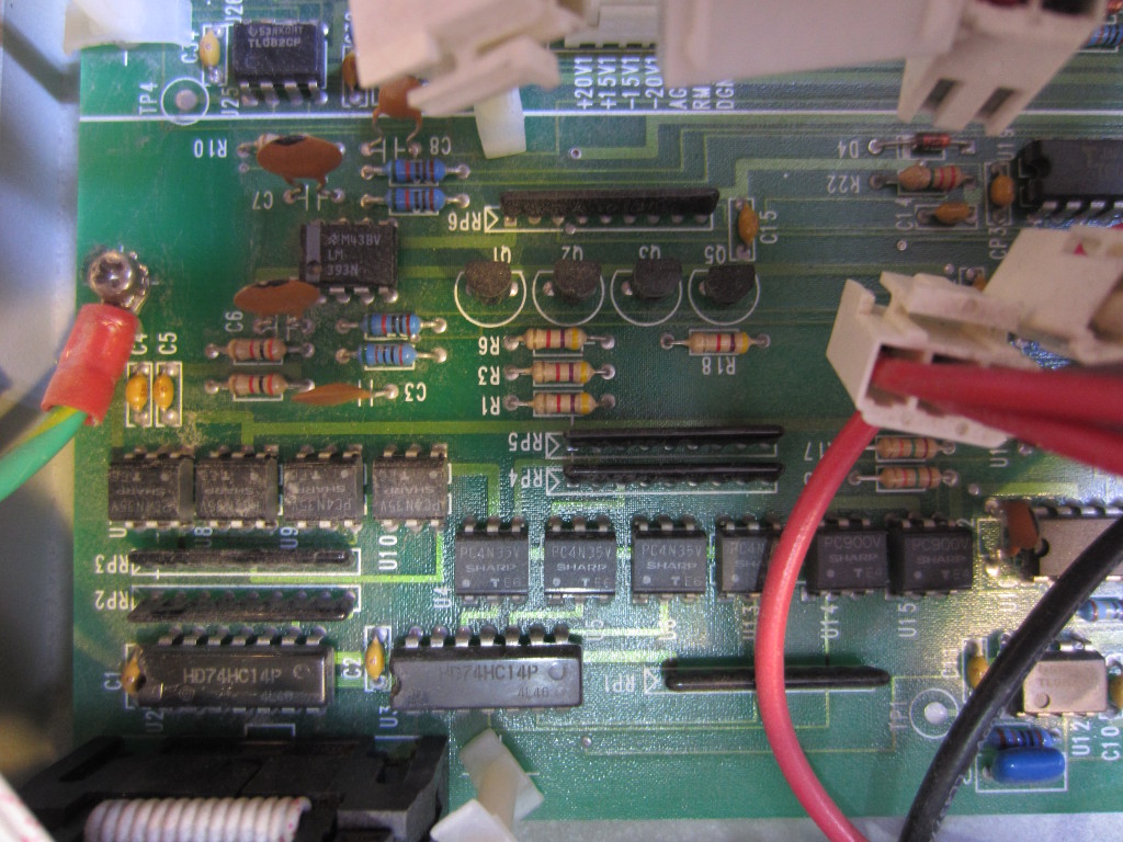
Everything on the digital board is powered by a linear regulator 7805. The entire processor board is isolated from the remaining power supply circuit via an array of optocouplers.
|
|
Clearly, this 74HC373 was not seated properly before the board was soldered, another chip on the main board also has the same issue. I am guessing that the pick and place machine must had some difficulty properly inserting these chips. On the back of the board, there are couple of bodge wires. Other than that the layout is pretty clean.
|
|
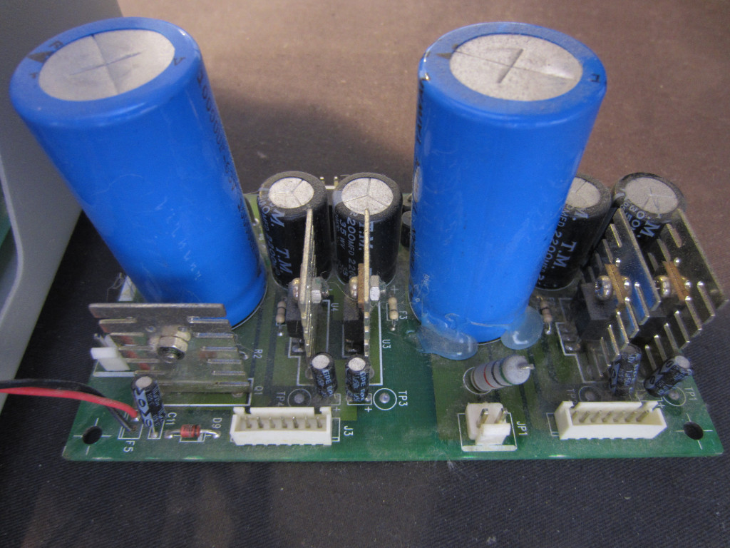
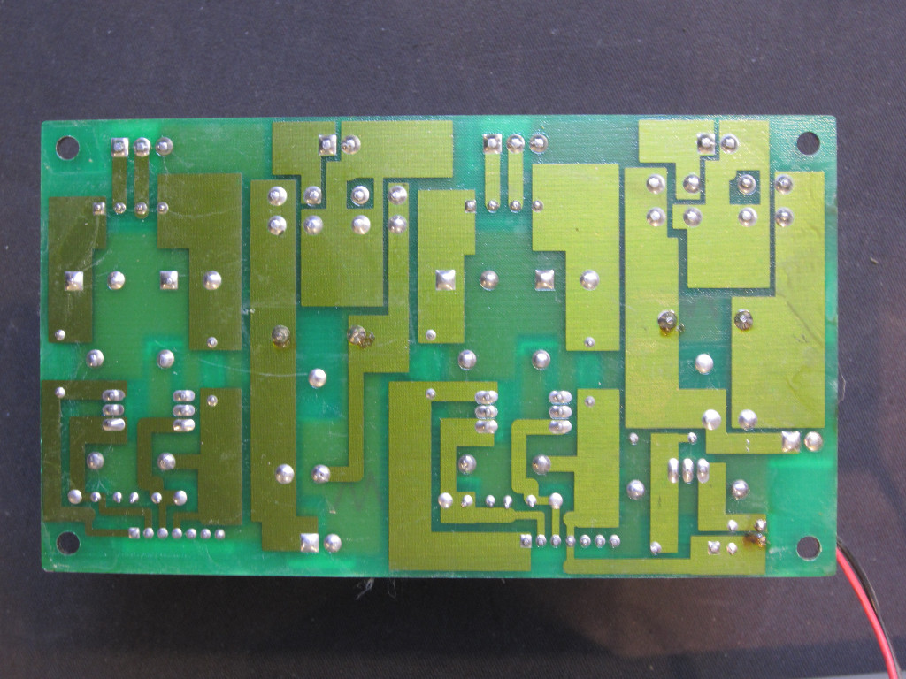
The auxiliary power supply board is fitted on four plastic standoffs above the main board. The two large filter caps are 10,000µF 63V each, although they are only rated at 85°C. Since the caps are placed far away from the main heatsink, I suspect that temperature wasn’t really a concern. Looking at the bottom of the board It seems that the PCB for the auxiliary power was designed by hand.
|
|
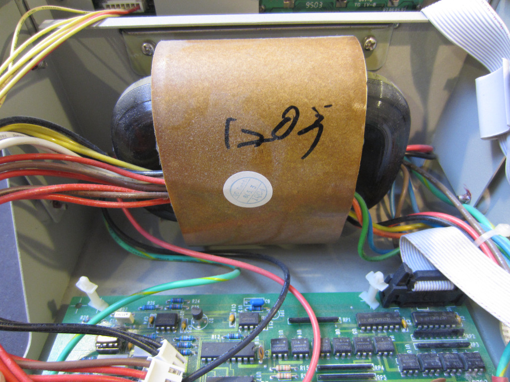
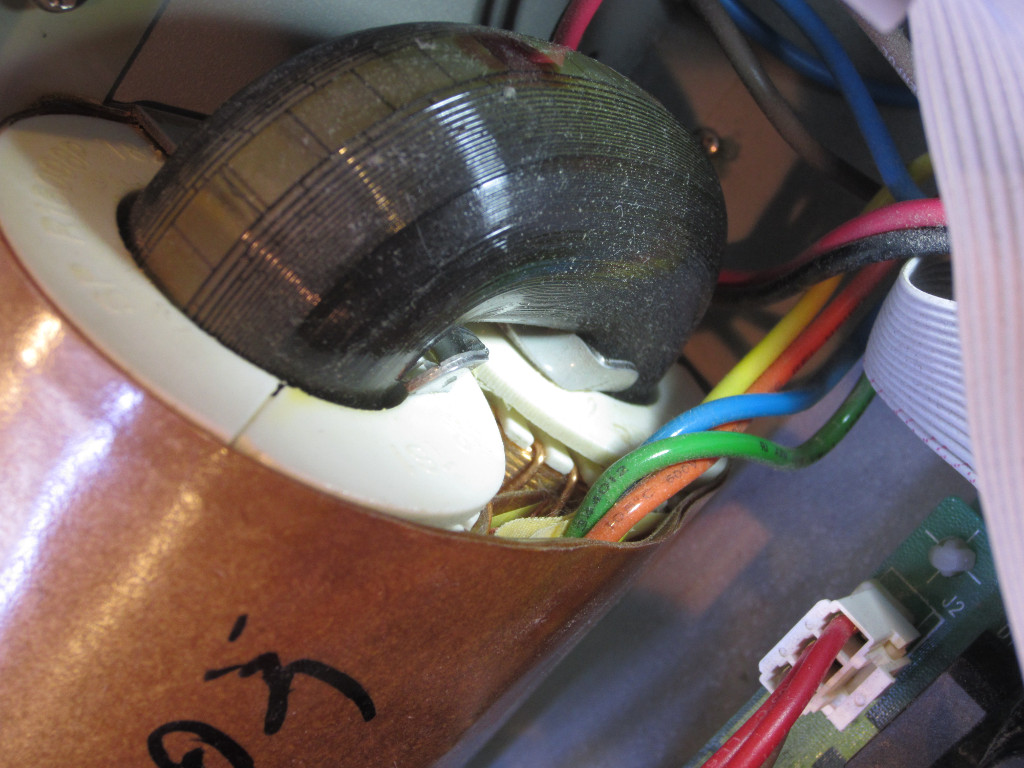
The C-core transformer is an absolutely thing of beauty, it is located towards the front of the unit. The reason for the placement of the transformer is mainly for weight balancing since the heatsink is located towards the rear of the case. Though the transformer is much heavier than the heatsink so the case feels a bit front heavy.
|
|
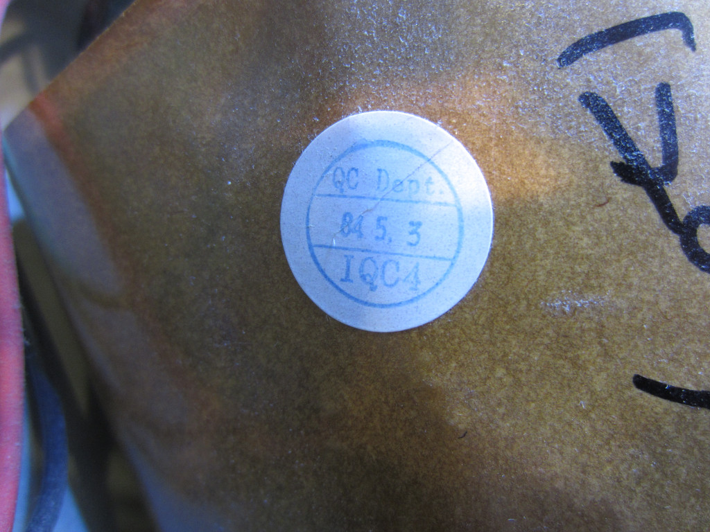
From the Q.C. sticker, it seems that this transformer was made back in 1984. Although the date codes on the ICs and the silkscreen suggest that this power supply was make in 1995.
I did not bother taking off the front panel as there wasn’t anything interesting besides a two line character LCD and a keypad. On the left below is a picture of the backside of the LCD, it looks like a pretty standard 16×2 LCD. The picture on the right shows the socket on the backside of the keypad board, a couple of keypad controller ICs are also visible.
|
|
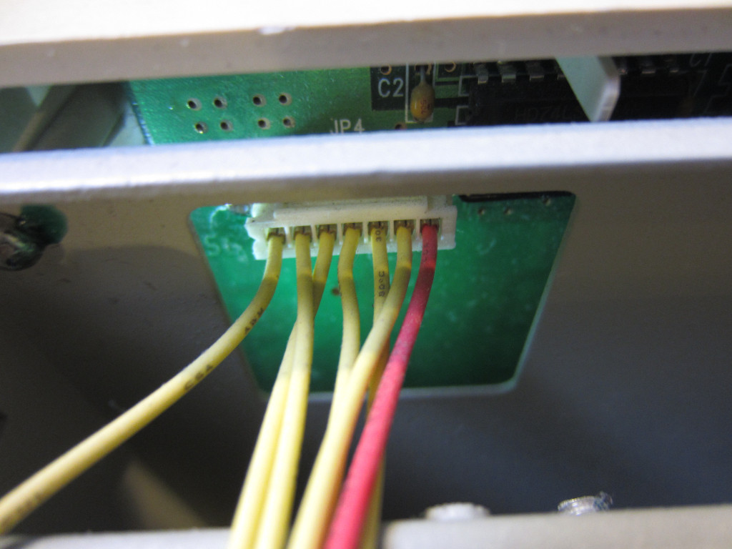
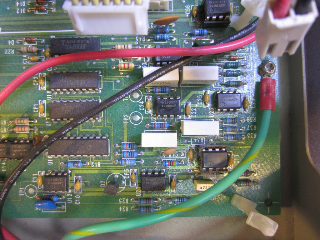
One thing interesting is how the wires to the front terminal posts are routed. If you follow the red and black wires from the front terminals you will see that they end up all the way at the back side of the power supply near the output terminal blocks. One issue to this layout is that because the wires are relatively long, the voltage drop across them can be quite significant. At full 2A load, the measured voltage drop approaches 10 mV at the terminals.
Since the front outputs do not have the sense terminal, you will need to use the rear terminal block connections in situations where higher precision is needed.
|
|
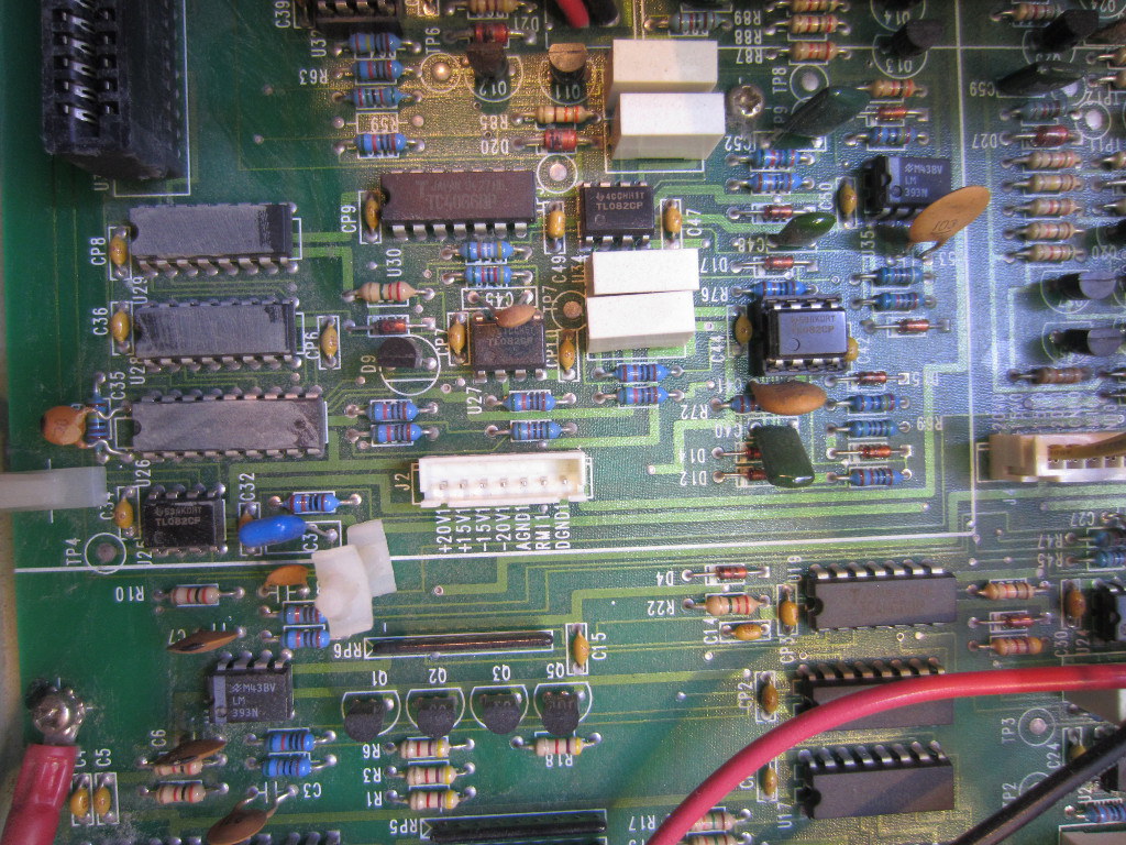
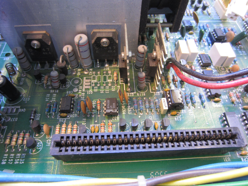
The two pictures below are the closeups the main board. In the left picture you can see one of the 74HC14 was not seated properly before soldered, similar to the problem we saw earlier on the processor board. And in the picture on the right, you can see all those 4N35 optocouplers similar to what you saw on the processor board. In a lab-grade programmable power supply, opto-isolation is critical as you do not want the power circuitry to destroy your entire system during a malfunction.
| [adsense] |
|
|
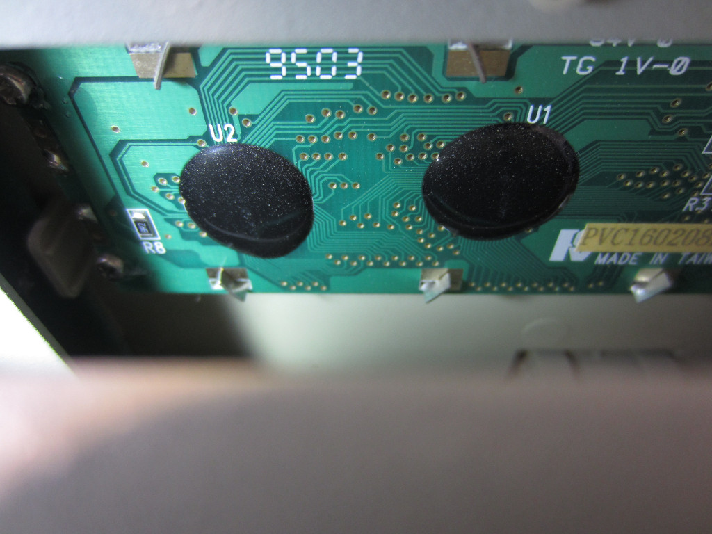
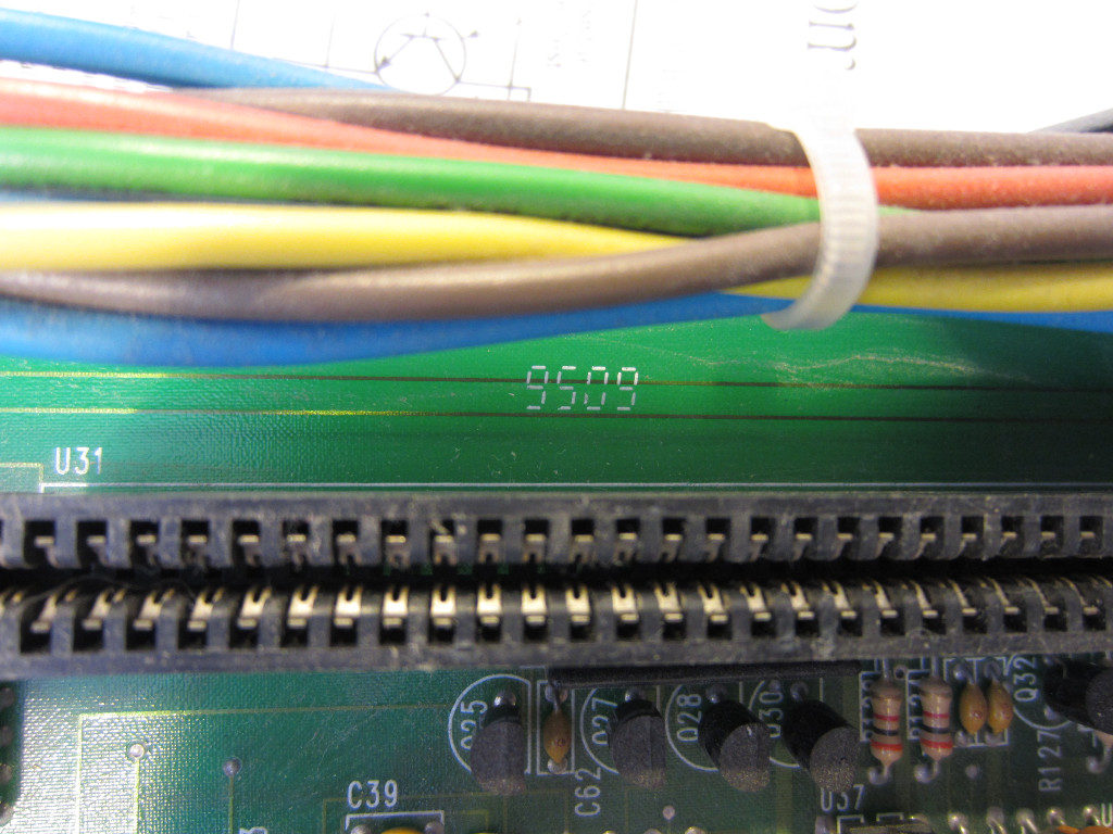
The picture below to the left is a shot of the processor board socket, you can see the date code (9509) on the edge of the PCB, which clearly indicates that it was manufactured in late 1995. On the other picture, you can see the DAC used in this PSU. It is an Analog Devices AD7541 12-Bit DAC. The output voltage resolution is determined by this DAC and at 4096 steps, the minimum adjustment interval for the output is just under 10mV.
|
|
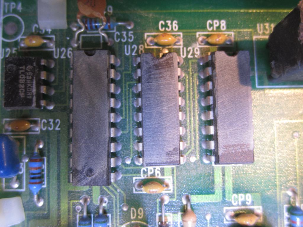
In this portion of the main board, you can see three ICs with markings sanded off. I am not entirely sure what these three chips are used for here but clearly it must be something Amrel thought was important enough to put the effort in to obfuscate.
|
|
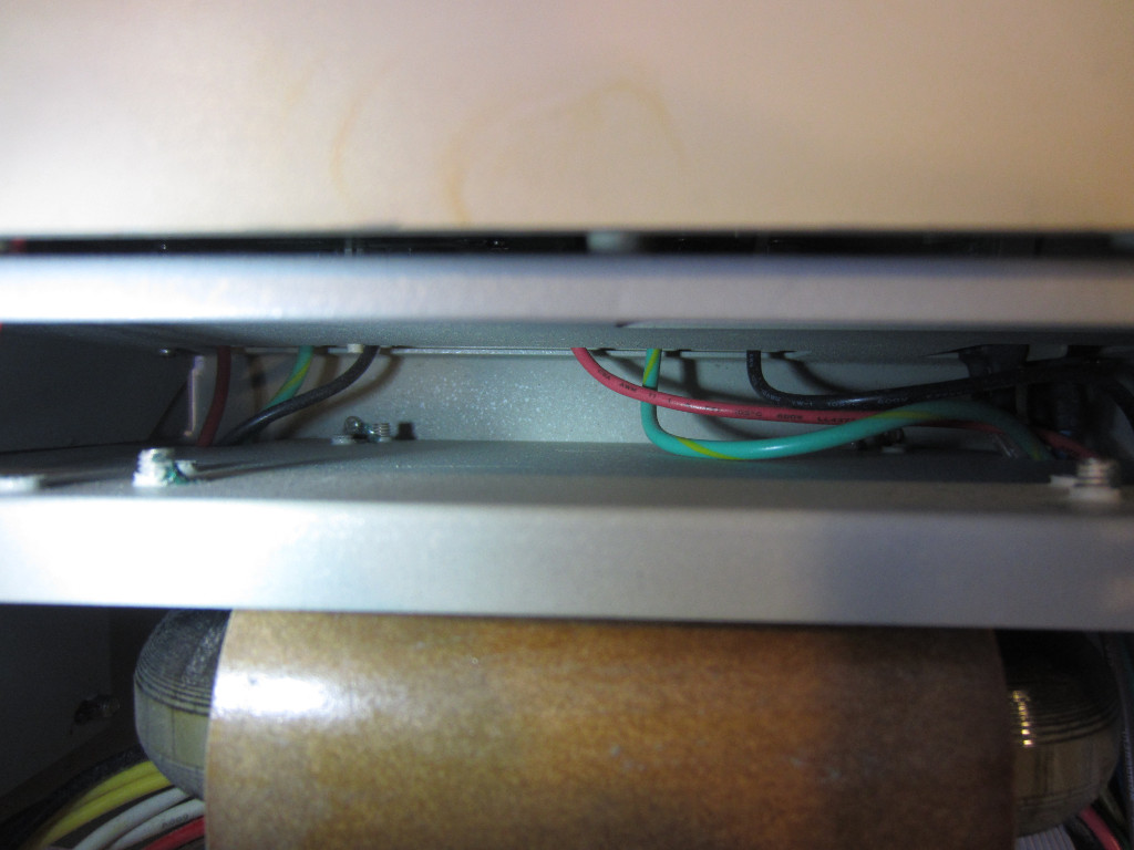
As mentioned earlier, the front panel binding posts are connected to the outputs all the way at the back of the unit, and here you can see the black and red wire running across the board.
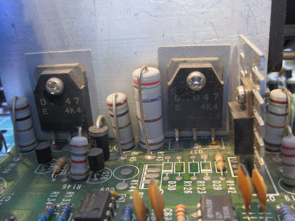
Here is a picture of two heat sinked power transistors (TIP31C and TIP32C). All heat sinks in this power supply are securely soldered on via multiple points.
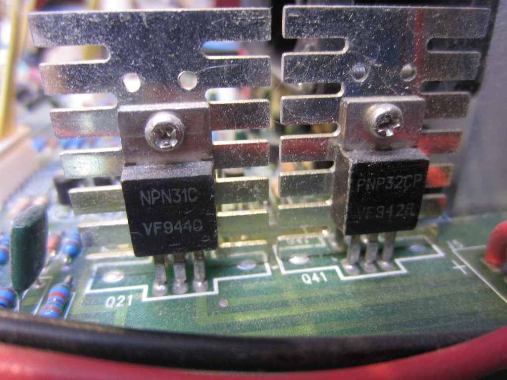
The pass transistors used in this power supply are 2SD1047‘s, two for each channel.
The main heatsinks (there are two, one for each channel) for the four 2SD1047s are rather small compared to the ones I saw in other power supplies. But they stay within the desired temperature even under full load thanks to the powerful cooling fan. Unfortunately, the fan is not temperature controlled and is always on. It is quite noisy.
I may add a fan controller to it (like I did with my Topward 6603A a few years ago) later.
|
|
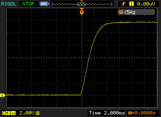
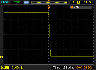
The oscilloscope capture below are the power-on and over-current protection characteristics. The power on voltage curve is nice and clean and over-current cut off looks quite excellent as well.
|
|
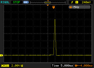
PPS-2322 also has over-voltage protection capability. Here is an oscilloscope capture of the OVP in action. The output voltage was set to 12V and the OVP level was set to 10V. The output was initially turned off and the waveform was captured when the output was switched on. As you can see when the voltage reached to around 10V, the output was automatically cutoff. The entire process took less than a couple of milliseconds.
One thing interesting about this power supply is that there is not a single relay inside. This means that there are no taps in transformer’s secondary to select from when the output voltage changes and thus the same input voltage is being bypassed via the power transistors at all times. So when the output voltage is low and when the current approaches the limit, each power transistor will dissipate more than 40W of power. But, as mentioned earlier the heatsink never gets really hot even under the maximum power dissipation.
At lower output voltages though, you do suffer the significantly decreased efficiency compared to other power supplies that select different windings depending on the outputs. But for a linear power supply, efficiency is not too much of a concern anyway.
Since there is no relay, the output on/off control relies entirely on the output transistor being turned on or off. In theory, the output on/off should be done using a relay since without a relay a connected device can inadvertently damage the power supply even when the output is off. But in practice, as long as you don’t try to connect a high voltage source to the output terminal when the output is off everything should be fine. In general though, you should never connect a low impedance voltage source to the output terminals of a power supply as most power supplies cannot sink current and doing so may damage the power supply.

