A while back, I did a teardown of an 800W Reliable Electric Pure Sine inverter. In this blog post, let’s take a look at a CNSWIPower 1500W pure sine inverter from Xijiatec.
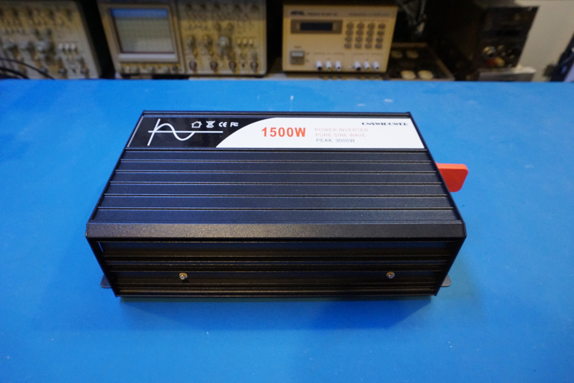
The version I received is a 12V one. The overall size of this inverter is only slightly larger than the 800W Reliable Electric inverter I have, coming at roughly 10.25’x6.5’x3.5′. It is however significantly heavier due to the additional components for the higher power rating. The case is made of extruded aluminum and it feels rather sturdy.
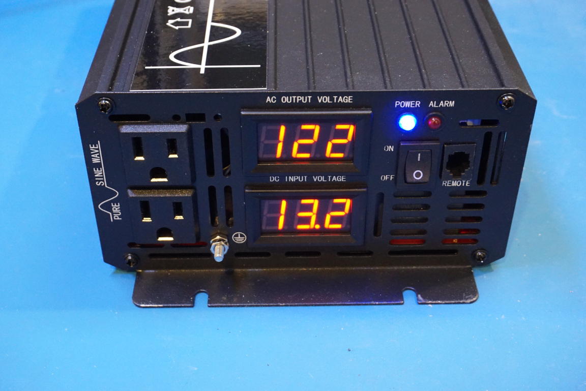
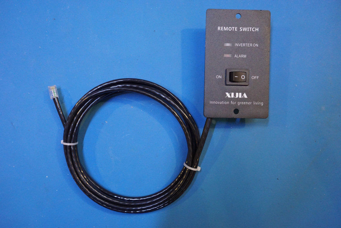
The front side of the inverter features two volt meters, one for displaying the current output voltage the other for displaying the battery voltage. There is also a remote control panel included in the package for fixed location installation.
The case employees a clam shell design. Once the screws on each end panel are removed, the top cover can be easily removed. As you can see in the picture below, the overall layout inside is relatively clean.
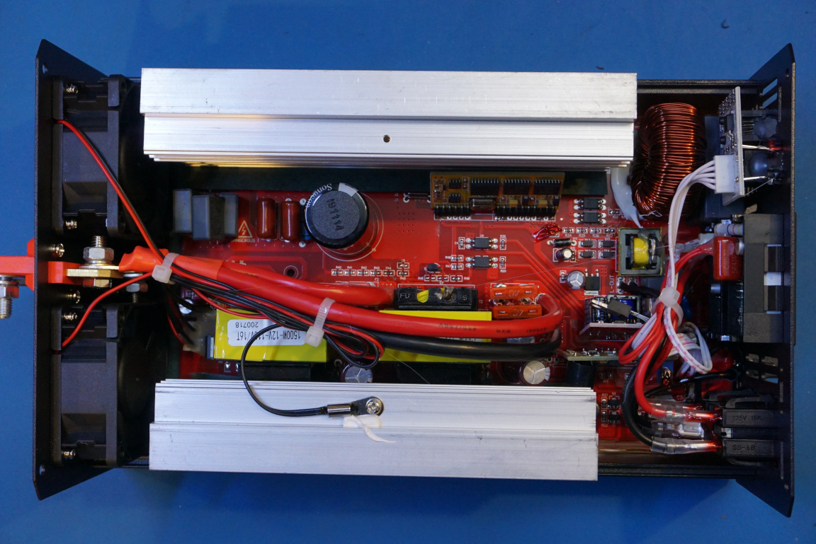
Here is a picture showing the bottom side of the PCB once the board is removed from the case. Although there are mounting holes on the PCB, they are not used. Instead, the assembly is secured inside the case via a few screws between the case and the aluminum heat sinks on either side.
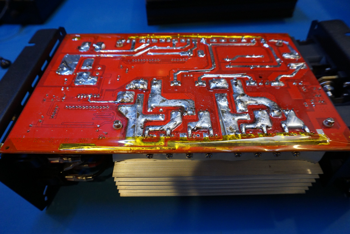
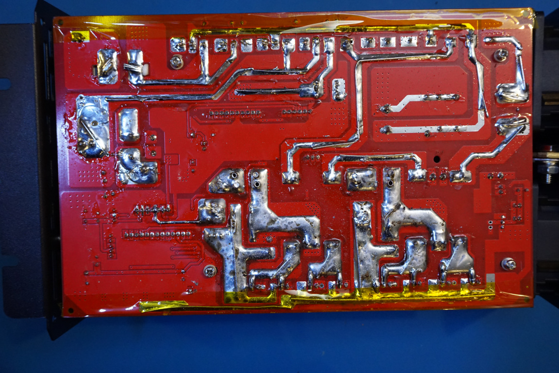
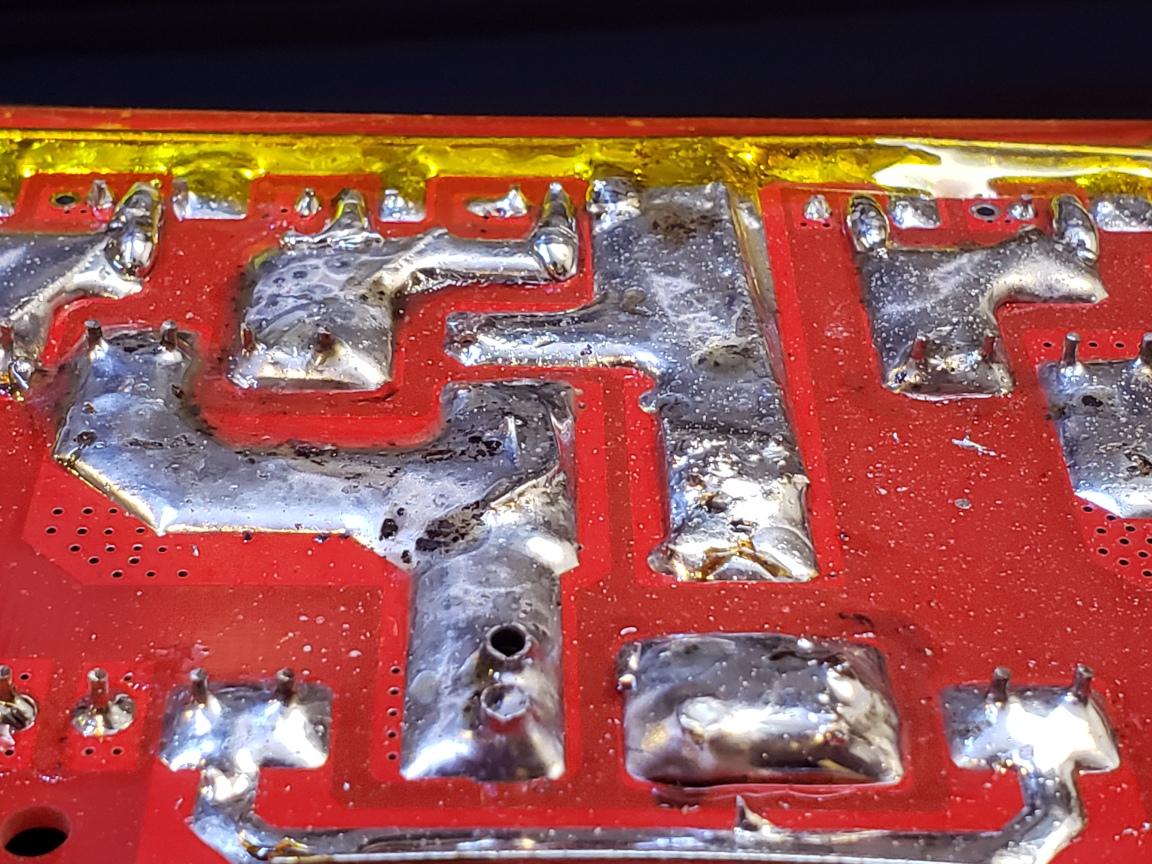
As you can see from the these pictures, the traces are heavily tinned to lower their resistances. Furthermore, additional wires are embedded in those high-current traces for added current carrying capabilities. This is not the cleanest design and also may not produce a consistent result due to the variance in soldering skills. For this kind of low input voltage high powered inverters, resistance along the high current paths play a big role in the overall system efficiency as at full output power over 130A of continuous current flows through the system and even one milliohm of additional resistance would mean over fifteen watts of wasted power.
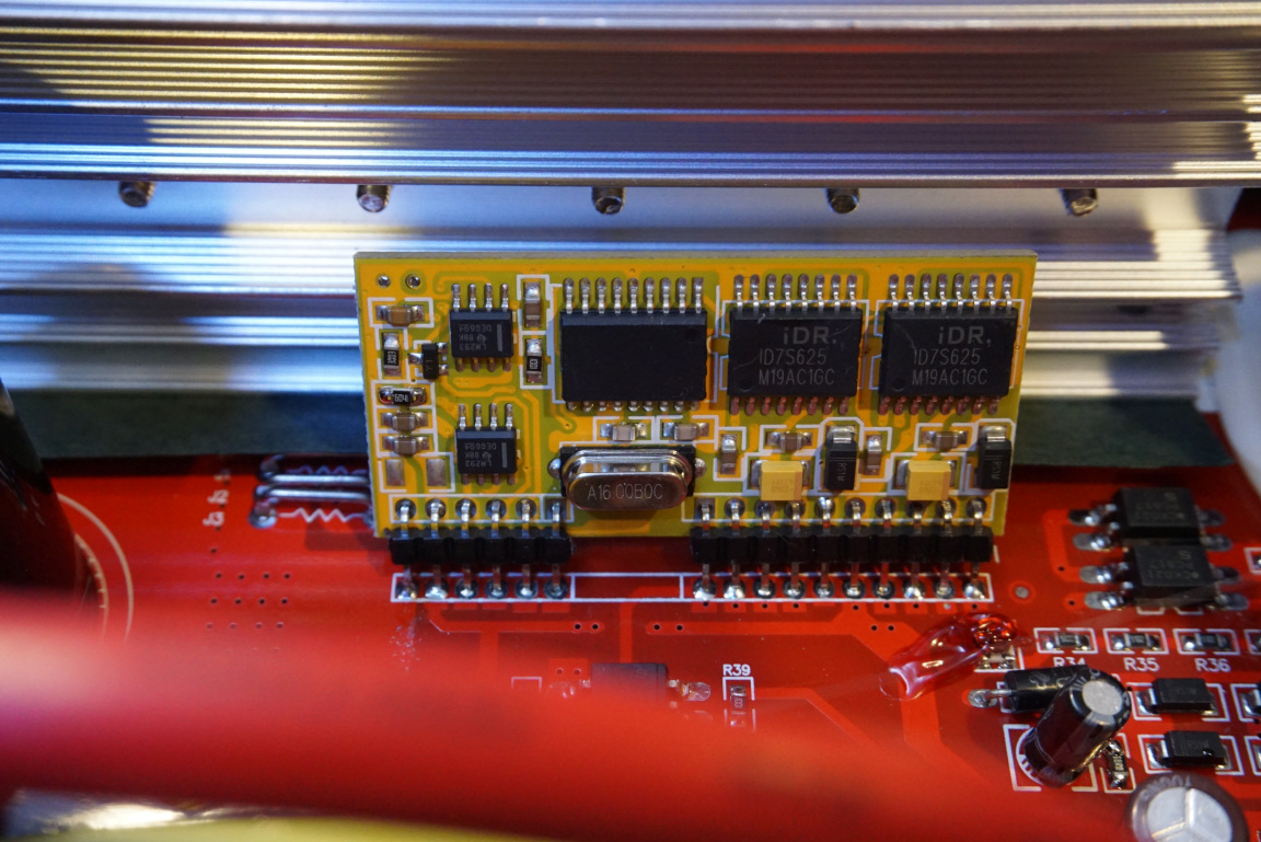
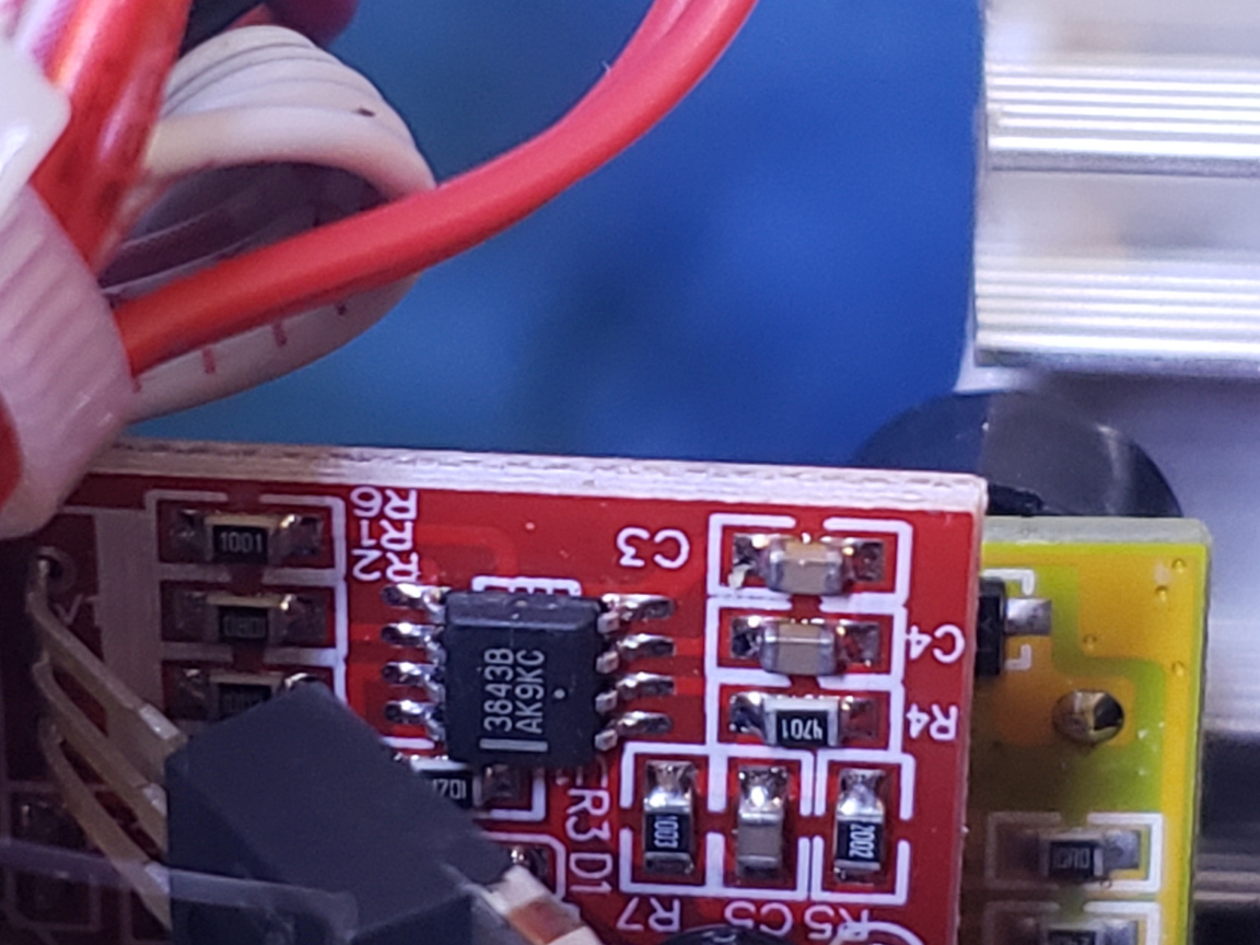
Like most of these pure sine inverters, the main controller circuitry is contained on a riser board. According to the user manual, the main chip is a custom chip (an ASIC?). I assume that’s what that chip on the left in the picture below with no marking is. I could not find any information on the other two ID7S625 ICs either.
The overall design uses a DC-DC converter stage to first step up the input 12V into a higher DC voltage (around 170V or 340V depending on the output stage design) and then a PWM signal drives the output bridge to approximate a sinusoidal waveform. Finally, the waveform is cleaned by an LC low pass filter to form the final output.
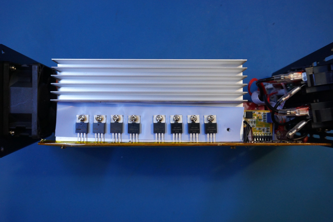
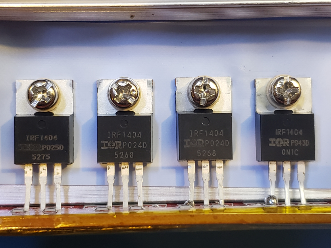
Below are a couple of pictures showing the IRF1404 power MOSFETs used for the DC-DC converter stage. Just behind the heatsink in the picture to the left below, you can see a small riser board (it has a piezo buzzer on the other side). According to the manufacturer, the trim pot on this board controls the overload cutoff point.
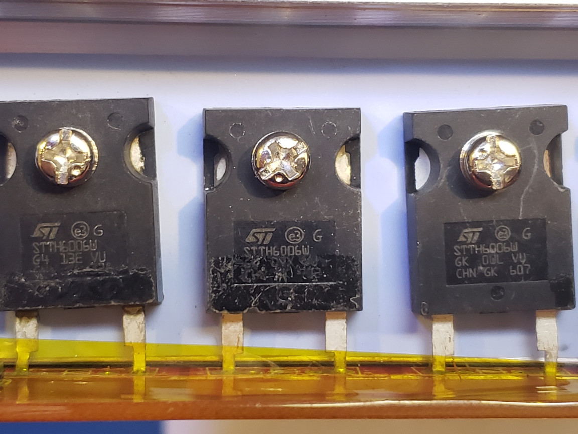
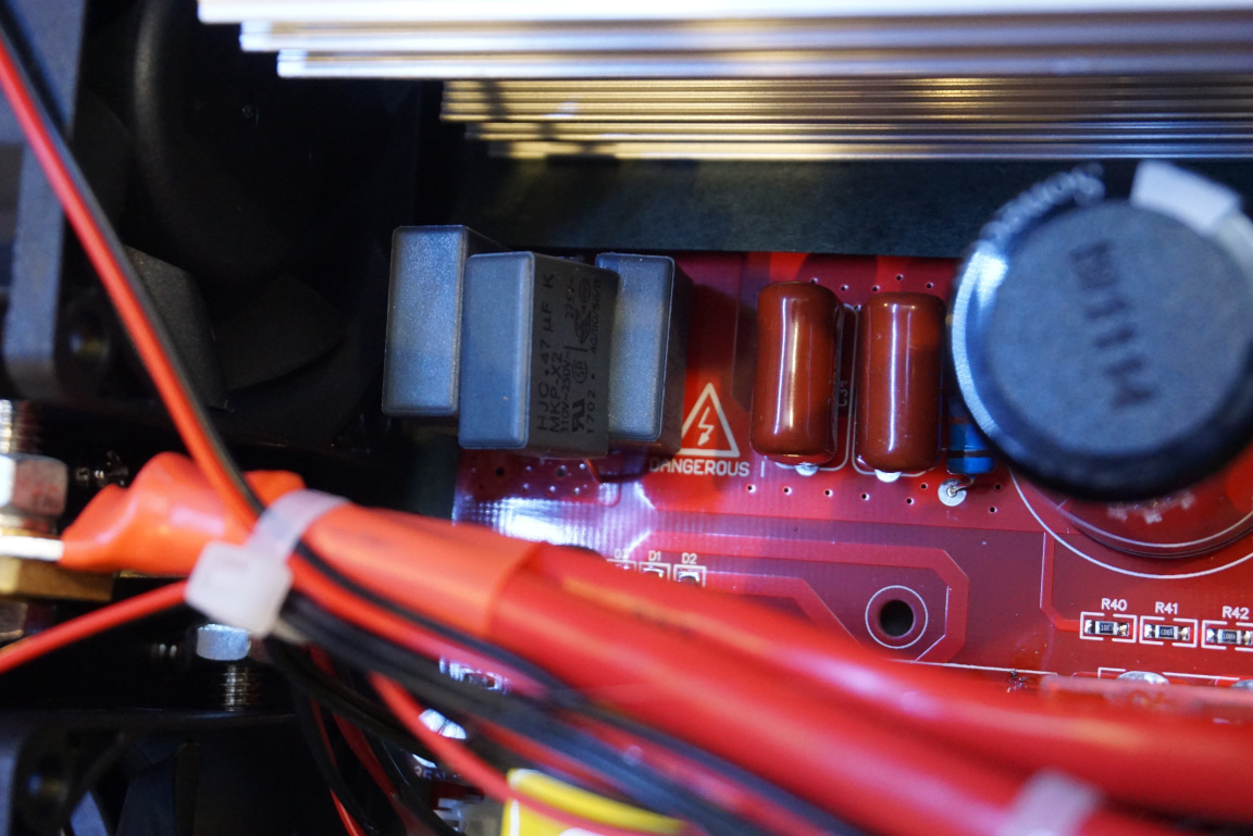
The picture to the left below shows the power devices used in the output bridge side. The picture to the right below are three of the four high voltage ultrafast diodes STTH6006W.
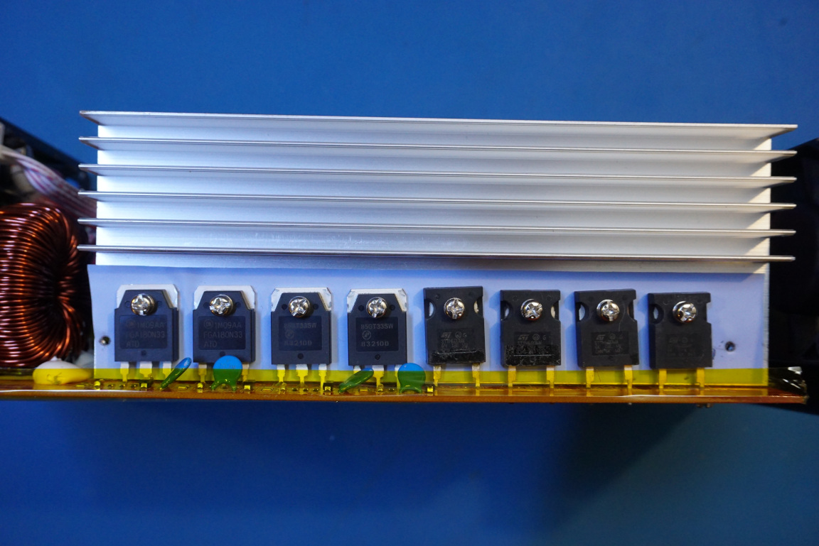
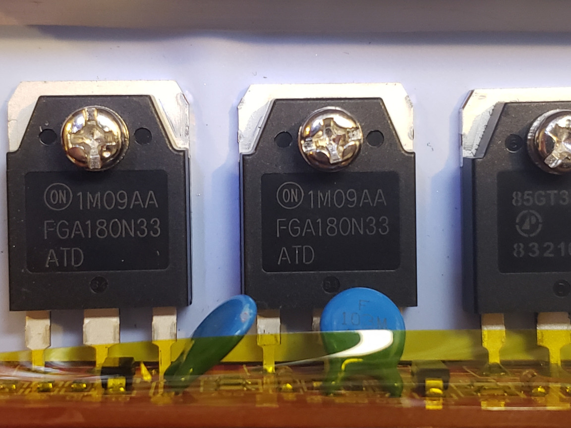
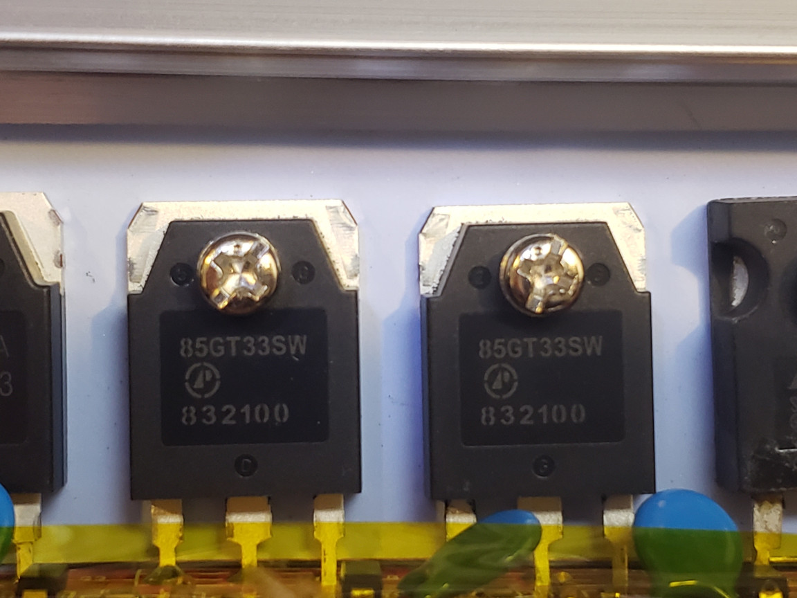
The power devices used in the output stage are IGBTs. The ones in the picture to the left below are two FGA180N33 330V 180A N-channel IGBTs. The other two are marked as 85GT33SW but I could not find any information on them. Since they are of a different model, I would assume that these are two P-channel IGBTs.
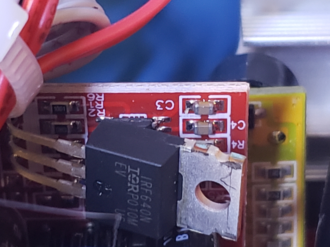
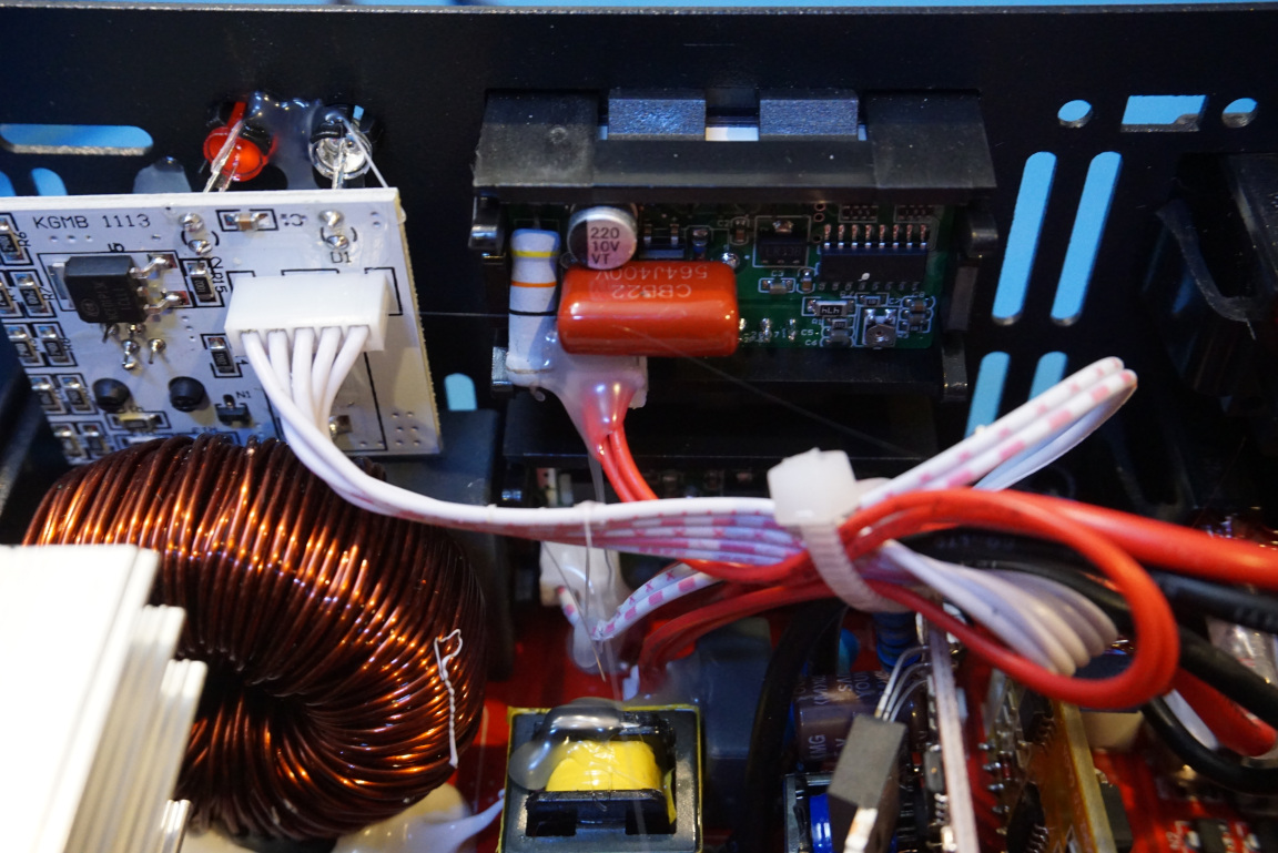
There is another riser board next to the riser board with the piezo buzzer. This one contains an 8 pin SOIC which I cannot find any information on and an IRF640N MOSFET. It also contains a small pulse transformer (not shown). So looks like it is a small DC-DC converter board, but I am not entirely sure the purpose of it.
The next three pictures from left to right: The first one shows the two pulse transformers used by the DC-DC converter. You can also see the above mentioned DC-DC converter riser board with the small pulse transformer mentioned earlier. From the picture in the middle you can see that the volt meters used are those off-the-shelf 3 ½ digit volt meters. If you look at the last picture, it appeared that the footprints for the capacitors do not quite match the physical sizes of the capacitors used, one of the capacitors sits above the others as it could not be squeezed in.
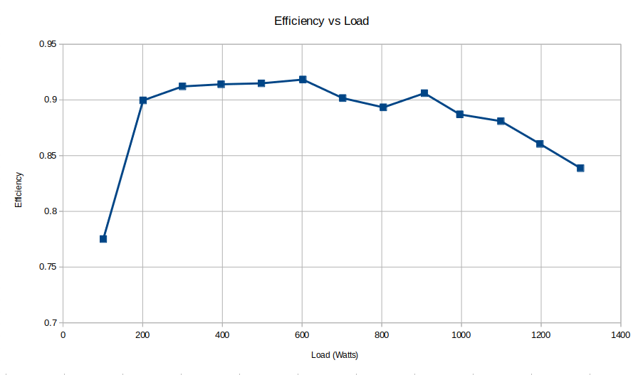
During the load testing, it became apparent that the 1500W rating is a bit exaggerated as the inverter would sound an overload alarm when the load exceeds 1300W and would cut off the output shortly afterwards (around 1350W in my testing). So clearly the maximum rated continuous power is over stated for this inverter. According to the manufacturer, the cutoff maximum load value can be adjusted via the trimpot on one of the vertical boards mentioned before. But I am wondering why they deliberately made the maximum wattage lower? Whatever the reason, it is perplexing that maximum load was factory set at below the rated wattage. With that said, the efficiency of this inverter is excellent.
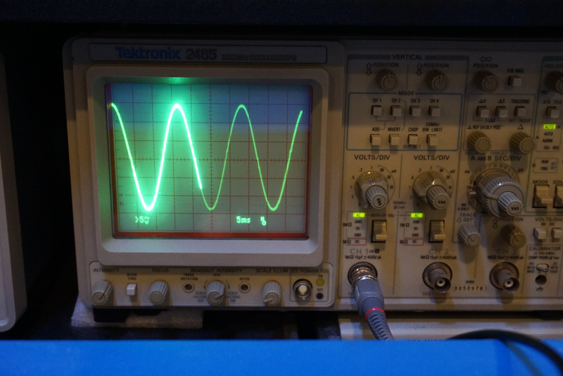
As a pure sine inverter, the quality of the output waveform is also very good. There is a little bit of distortion but the waveform quality does not seem to be impacted no matter how heavy the load is.
Perhaps more importantly this inverter offers great efficiency. As you can see in the figure below, the measured efficiency is excellent when the load is between 200W and 1000W. Under these load conditions, the efficiency is generally above 90%. With no load, the inverter consumes under 5W which is also quite impressive.
Also worth mentioning is that for this SWI inverter the earth ground is tied to the case and the neutral exhibits high resistance to the ground. Because of this, you can safely tie the neutral to earth ground without affecting the operation of the inverter. This means you can safely use this inverter to power your house using the existing wiring via a transfer switch.
In the video below, I did a thorough review of this inverter. The video also included load testing and detailed teardown..

