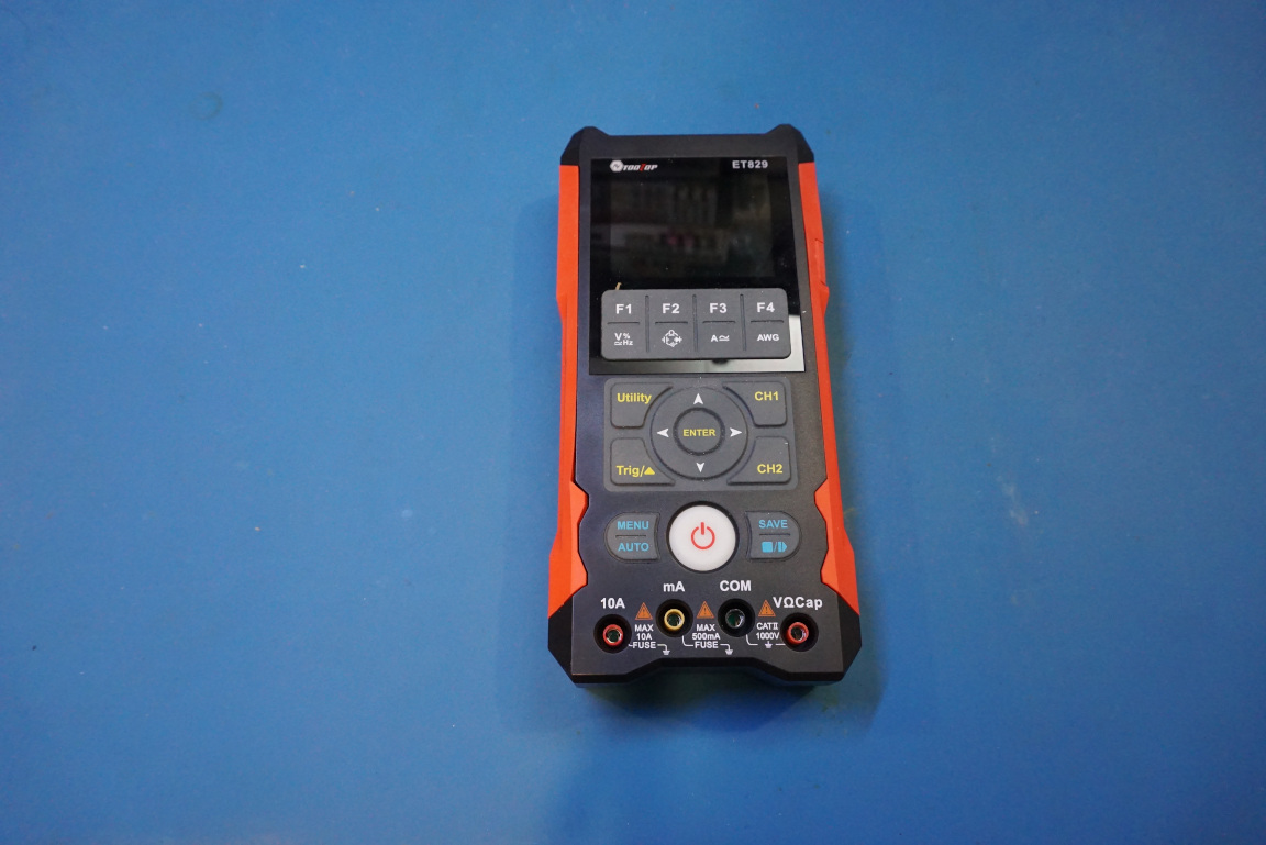
Over the last year, I have done teardowns of a few handheld scopemeters including a Hantek 2D72, an Owon HDS272S and an Owon HDS2102S. This time around let us take a look at this ToolTop ET829 3-in-1 handheld meter that I did a review video on last week. The ToolTop ET829 is essentially a 3-in-1 device boasting an 80 MHz bandwidth dual-channel oscilloscope, a 6,000 counts multimeter and a function generator. A video of this teardown is linked towards the end of the post.
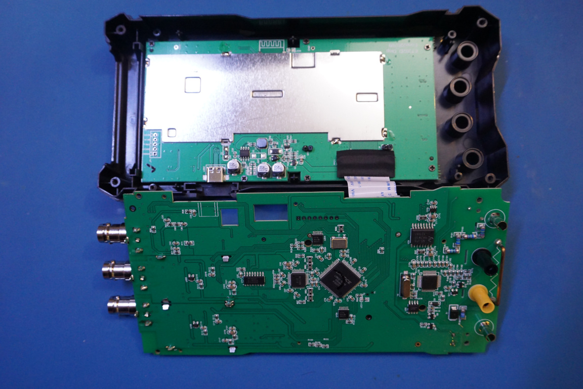
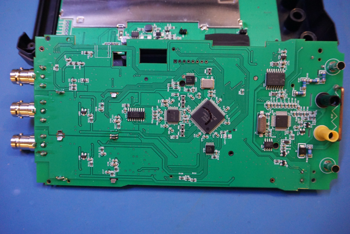
After removing the back cover, you can see the back side of the main board. Like the Owon and Hantek handheld devices, the ET829 is also powered by two 18650 lithium ion cells. From the board cutouts you can see that the ET829 also utilizes a two board design.
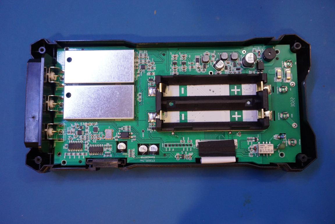
The top PCB unfortunately is soldered onto the bottom PCB via two header pins (you can see these two soldering points below the battery footprint near the polarity signs). In the picture below, you can see I desoldered on of the connecting pins so I could free the upper board. Note that the marking on the board says ET202D. I did a quick search and it appears that there are also similar handheld scopemeters on the market sold under the ET202D model number instead of the ET829 we see for this ToolTop branded meter.
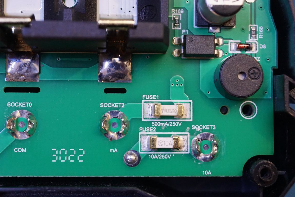
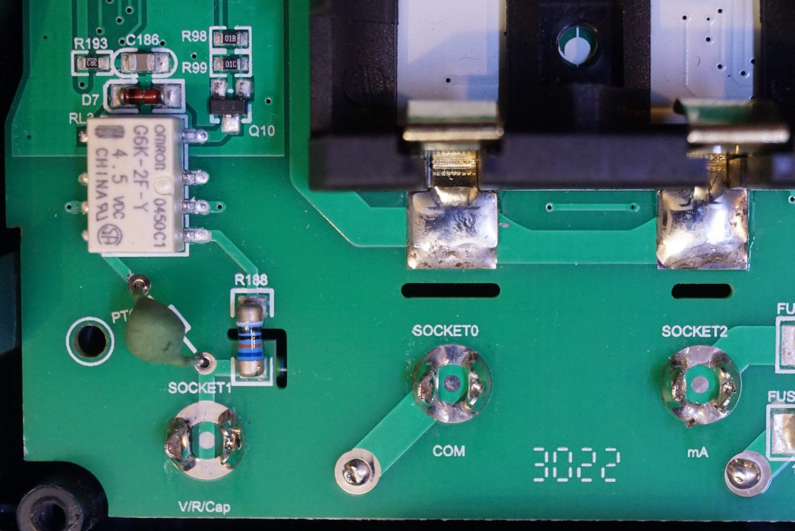
Below are a couple of close up pictures of the DMM input section. There are two soldered-on fuses for the current measurement ranges and a single PTC for the main probe input. There is no MOV protection however.
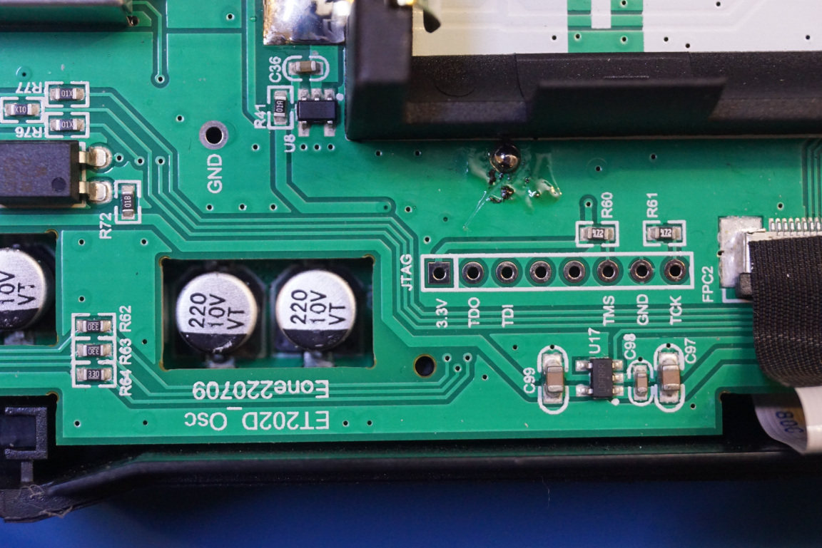
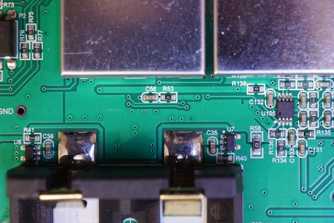
The shielding cans for the channel one and channel two input sections are unfortunately soldered onto the main board, so I did not take them out. The section in the picture to the right below is near the signal generator output. There are a couple of 74HC4051 multiplexers. The 8 pin SOIC chip to the left is a GS8092 rail-to-rail OpAmp which has a bandwidth of 350 MHz.
As mentioned earlier, the two boards are soldered together via two header pins. By the look of it, at least one of the header pins is for ground connection. This design in my opinion is unnecessary as the top board is securely screwed on, the two boards could’ve simply be mated together if needed instead of being soldered together.
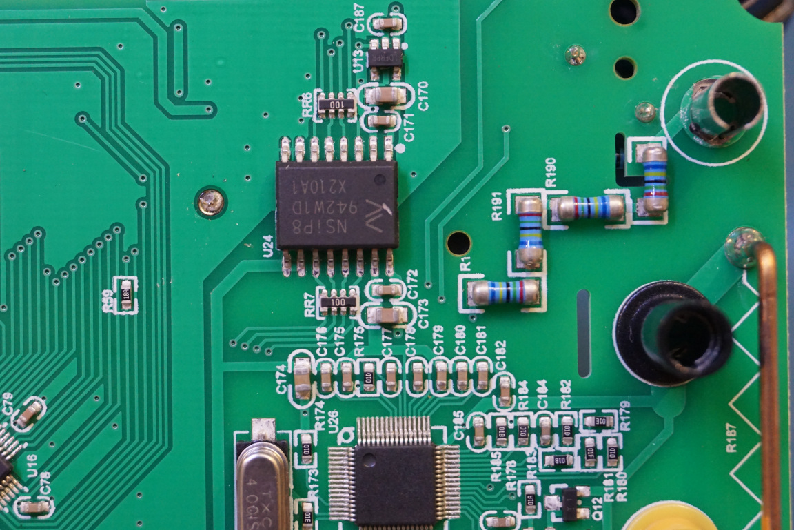
Here are a couple of pictures showing the DMM section. There’s no marking on the main DMM chip unfortunately so I couldn’t tell which chip set they used for the multimeter. I also could not find any datasheet on the chip marked NSiP8 942W1D. Given that we saw in either Hantek or Owon’s designs there are some opto-isolators in their DMM sections, could this chip be some kind of integrated multi-channel opto-isolators?
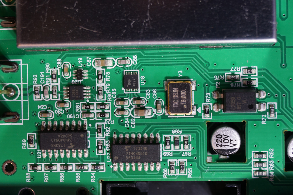
The FPGA used in this ET829 is a Lattice LCMXO2-1200HC chip, which has 1280 logic elements. This is essentially the same FPGA used in the Hantek 2D72. The ADC used for the oscilloscope input channels is an MXT2088 8-bit dual channel 100 Msps analog to digital converter chip. This is the same chip used in the Owon HDS272S. It makes sense as the maximum sampling rate of ET829 is 200 Msps when a single channel is in use and this rate halves to 100 Msps when both channels are used. The sampling rate for the Owon HDS272S is spec’d at 250 Msps however, perhaps the ADC is overclocked in that design.
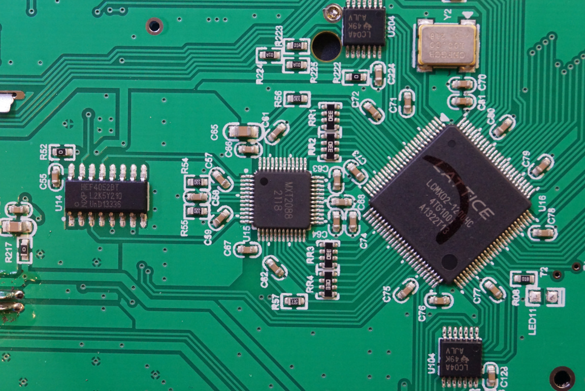
Unlike the Owon or Hantek designs, there is no dedicated DAC on this board. The omission of the DAC explains why the amplitudes of the signal generator output can only be set at discrete levels.
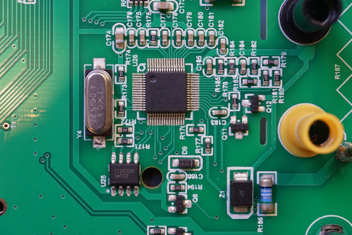
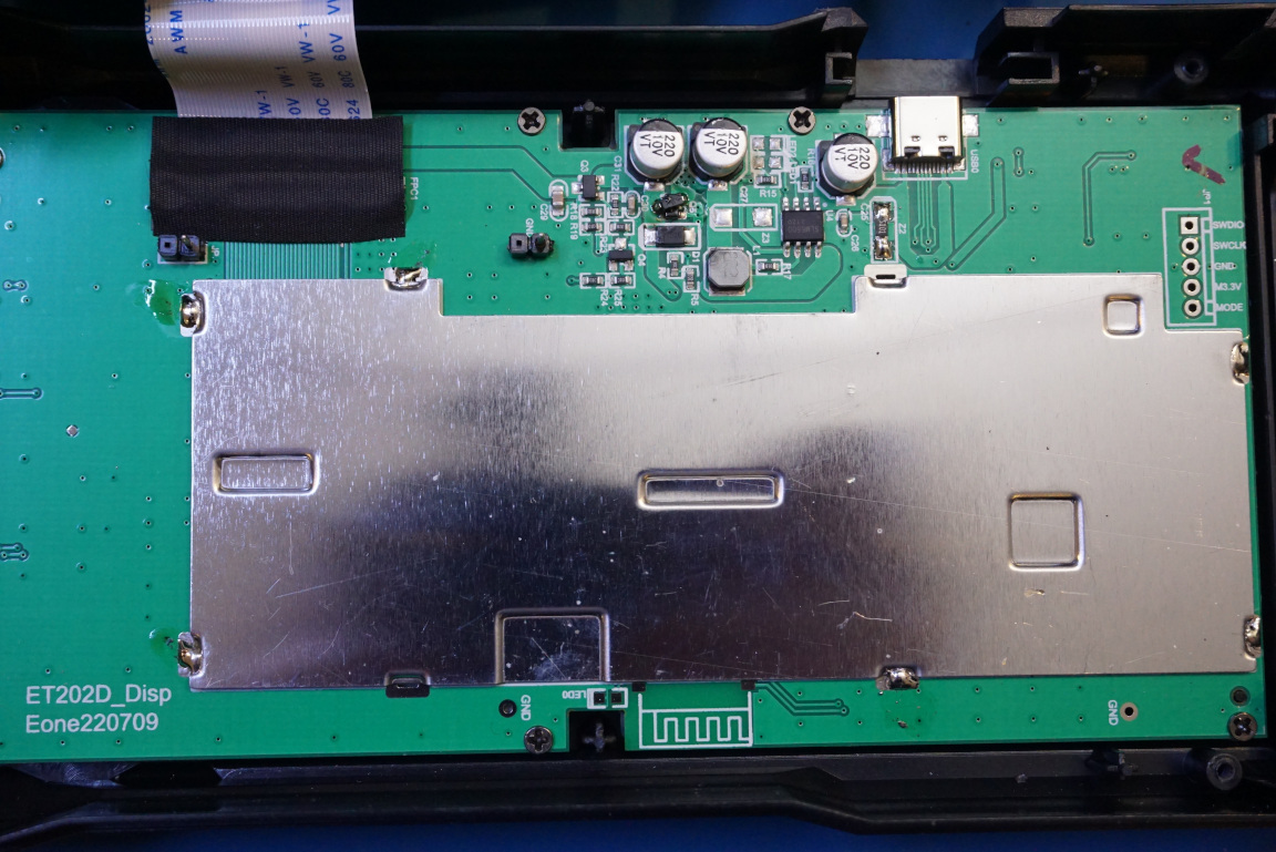
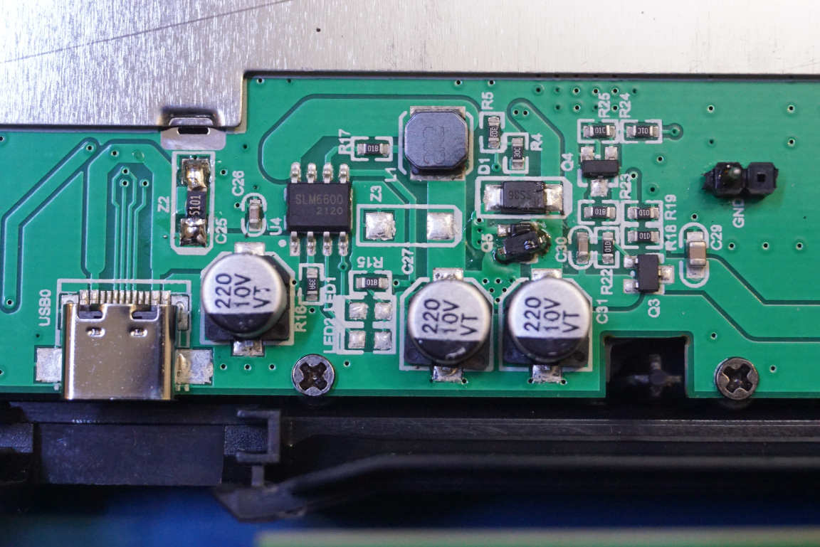
Below, you can see a couple of pictures of the front panel PCB. This PCB contains the display/keypad controls. There is likely a dedicated MCU on the other side as suggested by the programming header footprint. Interestingly enough, this board is also marked as ET202D as we saw on the main board. The picture to the right below shows the close-up of the battery charging circuitry. The charging controller is an SLM6600. If you look carefully, you can see there is a bodged on diode on Q5.
The video of this teardown is linked below:

