About a year ago, I bought a Cel-Fi Go X signal booster for my house as where I live the signal reception is very poor. I managed to do a quick teardown and examined the top side of the circuit board. But I did not take the board out to see the reverse side as in order to do so, I would need to desolder the SMA and power connectors. And that had left a lot to be desired.
After a year’s use, I have to say I am very impressed with its performance. Not only I have strong cell signals everywhere in the house (including the basement where I do most of my work from), I can also use my phone as hotspot when the internet is out and carry on a video conference without any issues.
So I was excited when I got my hands on another identical used unit. And this time around I was going to to do an extreme teardown and take a deeper look at the unit.
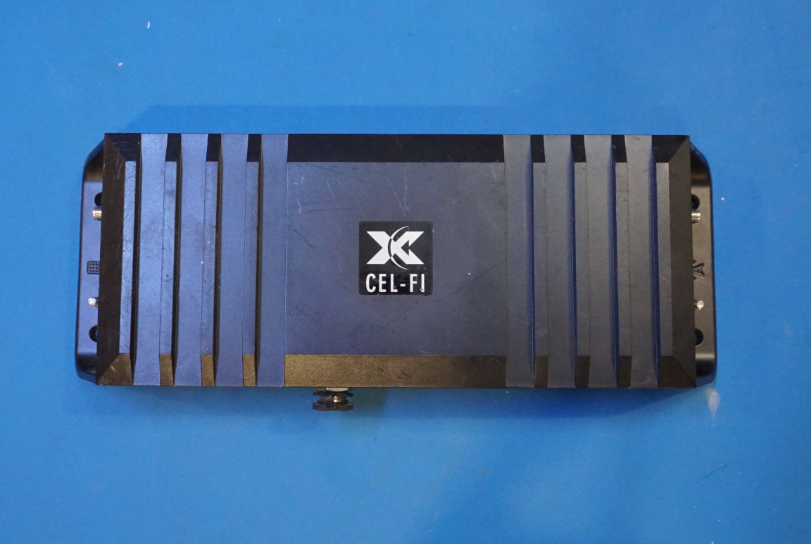
This used booster looks a little beaten-up from the outside. The only slight difference between this one and mine is that on each of the mounting bars there is a mounting screw, although it could have been added by the original owner.
The top cover is plastic as the Go X uses bluetooth to talk to the cell phone application for bi-directional communications. In the picture to the right below, you can see both the uplink RF section and downlink RF section with the shield cover removed. The uplink section is to the left which connects to the donor antenna, and the downlink section is to the right which connects to the broadcast antenna and communicates directly with the cellphones within range.
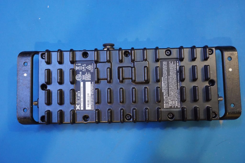
Judging from the serial number, this unit was made earlier than mine. But the inside looks pretty much identical. Because the unit is designed for outdoor use you can see the o-ring lining around the case opening.
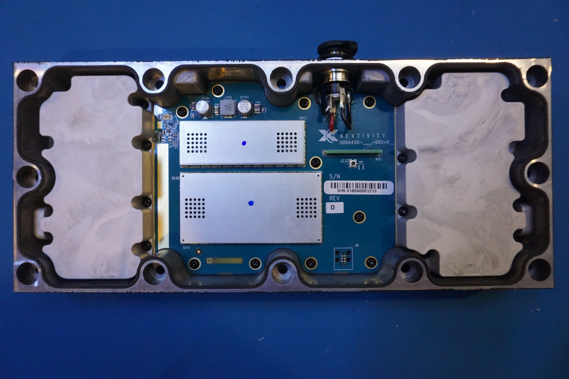
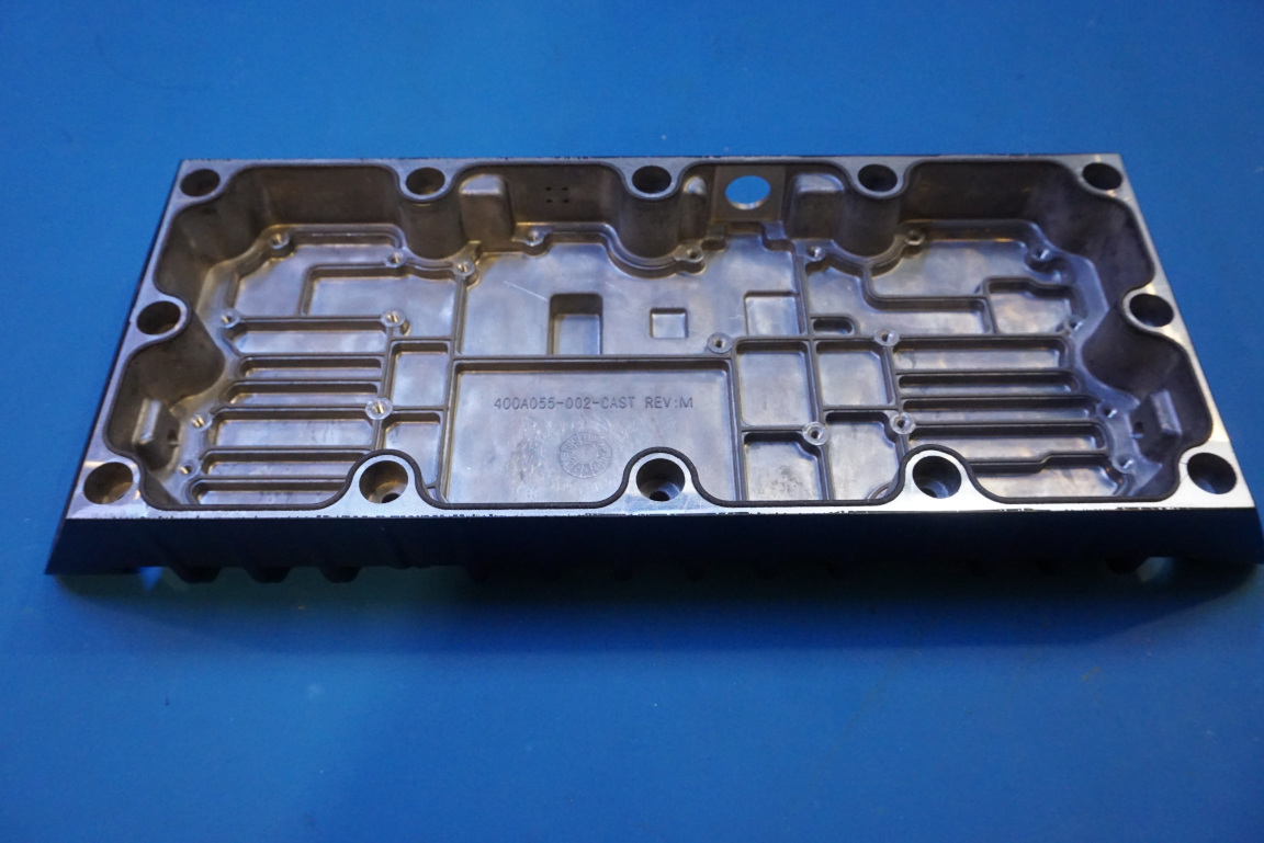
To get the PCB out of the enclosure, I had to desolder and remove both of the SMA connectors and the power connector. Upon removing the board you can see that the case is made of a single piece of die-cast aluminum. Each of the compartments is mated to the bottom side of the PCB via some RF gasket material, creating shielding necessary for each section of the RF circuitry.
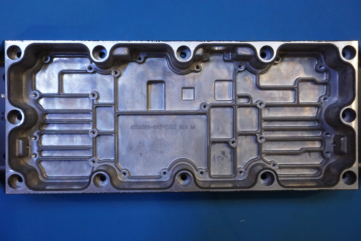
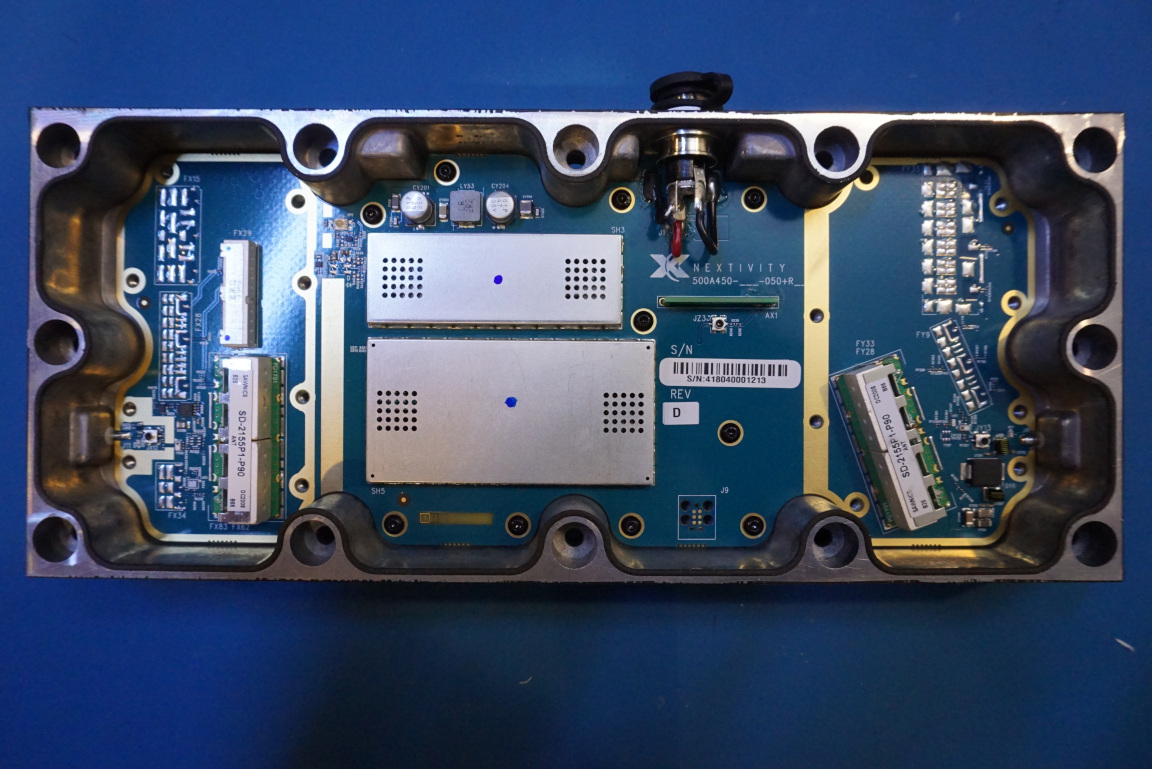
Besides the two larger shielding cans towards either side of the board that are screwed on, there are also two smaller shielding cans that are soldered directly onto the PCB. Removing them them undestructively proved to be difficult and I had to resort to brute force by yanking them off while using a hot air gun to desolder the cans one section at a time. During the process, I probably used a little too much force as I tore the PCB layer around the first section of the DC-DC converter as you can probably see from the picture to the left below. Also one of the electrolytic caps is knocked out of of place by the heat gun.
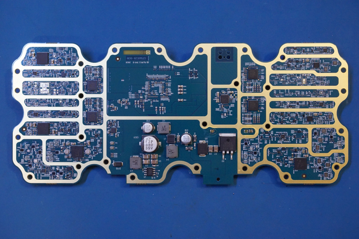
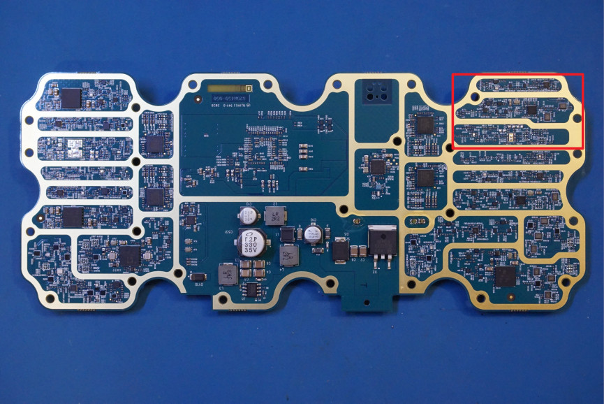
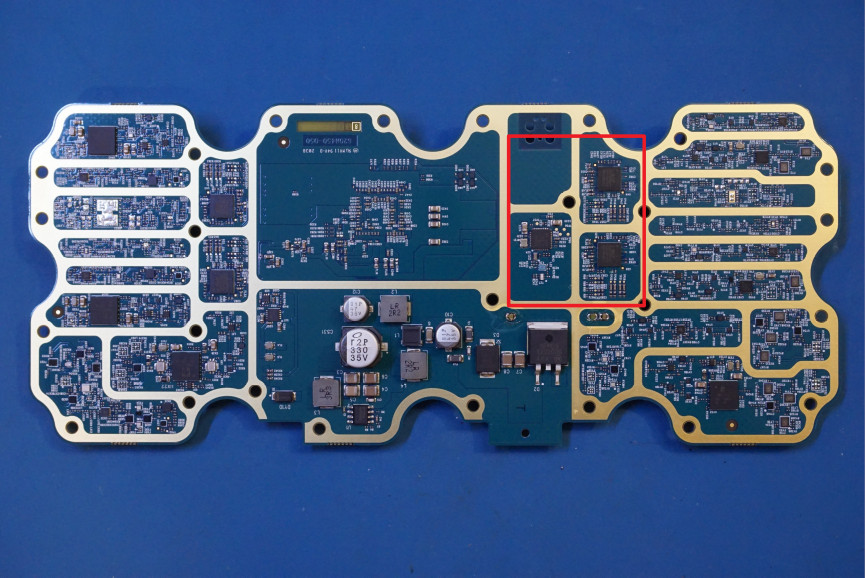
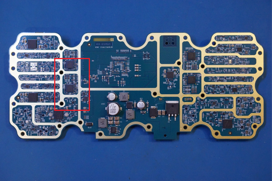
Here you can see both the top and bottom sides of the board in its entirety.
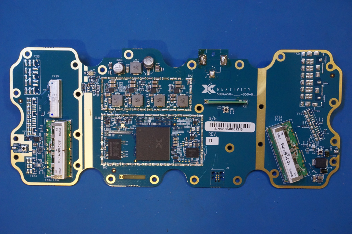
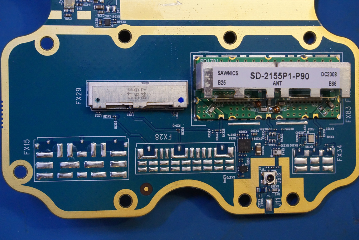
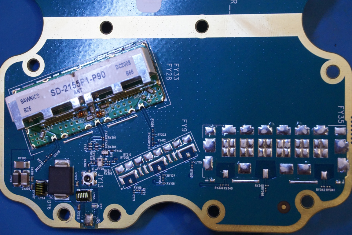
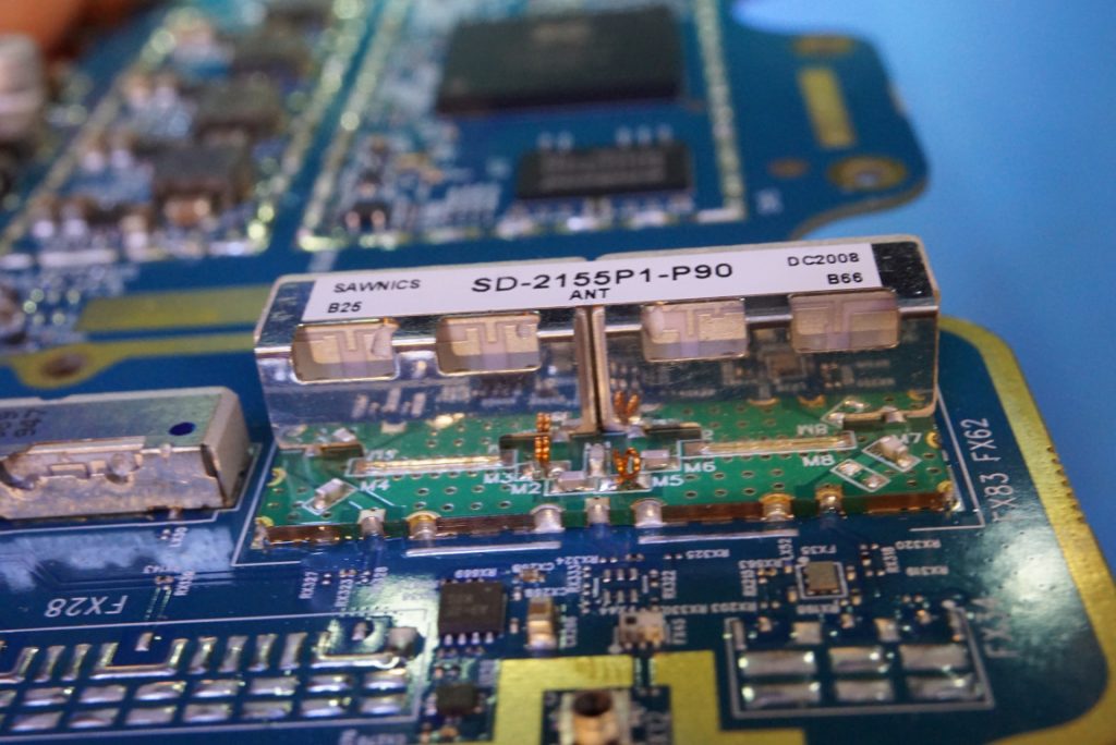
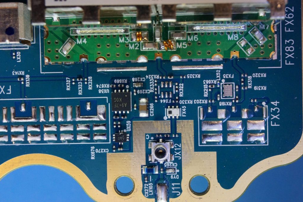
In the picture to the left below, you can see the topside of the uplink RF section. And the picture to the right shows the downlink RF section which connects to the indoor broadcast antenna. The two SAWNICS components (SD-2155P1-P90) are likely duplexers used to multiplex each antenna for both transmitting and receiving signals. The component next to the duplexer in the picture to the left below is likely a SAW filter.
There are a few unpopulated footprints on either side, these are probably reserved for similar duplexer/filters for different frequencies as the Cel-Fi Go X has other models that cover different frequency bands.
Here are a couple of close-up pictures showing the duplexer and the RF circuitry of the uplink RF section which communicates with the tower. In the picture to the left, you can clearly see the filters etched onto the PCB inside the SAWNICS duplexer module.
You can also see an UMCC connector along the antenna signal path. It is probably used during board level functional testing.
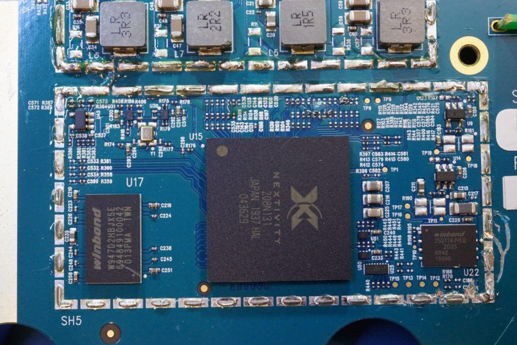
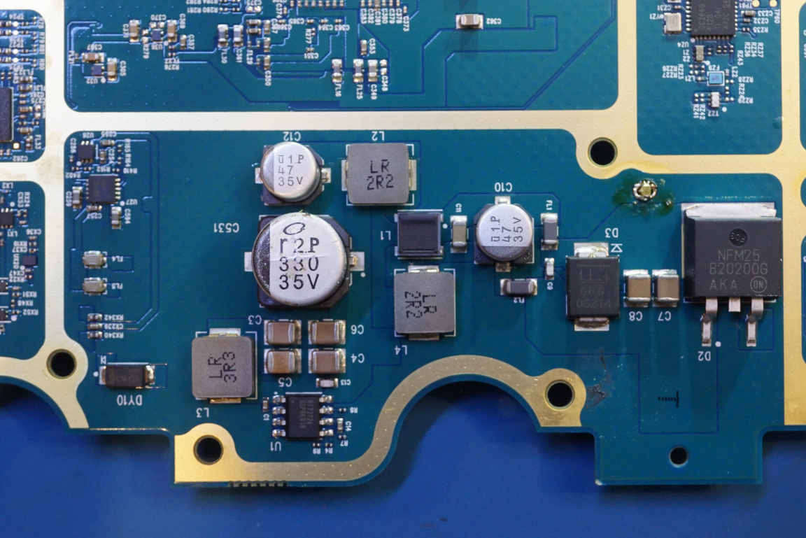
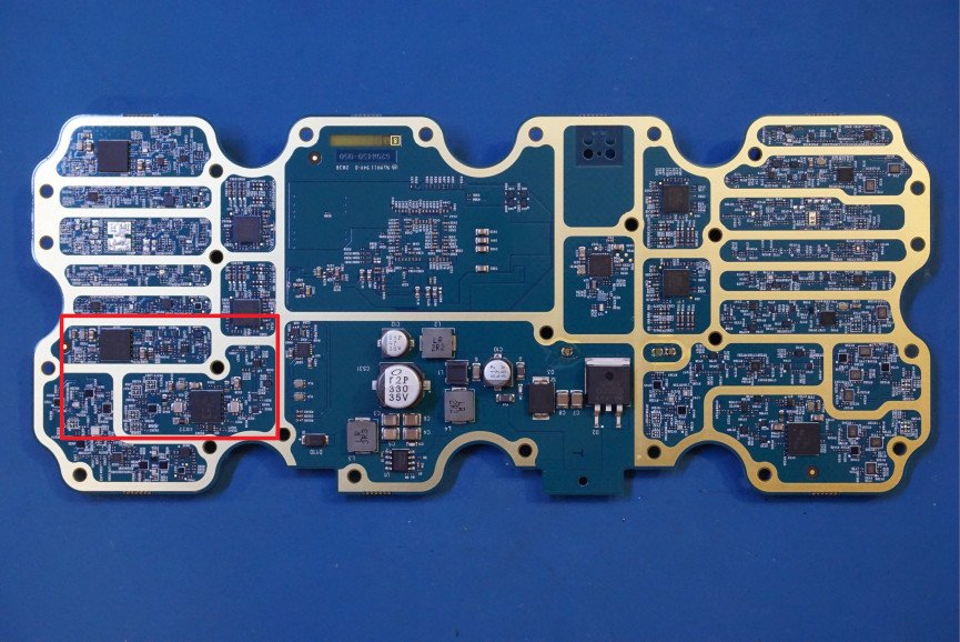
With the shielding covers removed, you can see the DC-DC converter section and the processor section just below it in the picture to the left below. There appears to be four independent DC-DC converters that are used to generate four different supply rails.
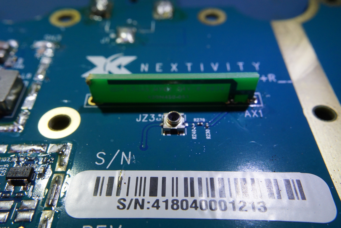
A close-up picture of the inverted F antenna used for the bluetooth communication can be seen in the picture to the right below. There is another UMCC connector there, which again is probably used for testing. You might be able to hook up an external antenna if you wanted longer bluetooth range. But in my previous testing, the bluetooth range is adequate in a multi-storied house for monitoring and controlling the signal booster.
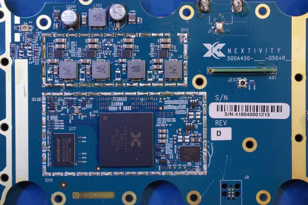
Here is a close-up of the processor section. The main chip is a proprietary Nextivity chip. I could not find any information on it. But judged by the number of supply rails used, it could be an FPGA or ASIC of some sort. The chip to the left is a Winbond W947D2HBJX5E LPDDR DRAM. and the chip to the right is a Winbond 25Q128JVEQ serial flash memory that sores the firmware and OS.
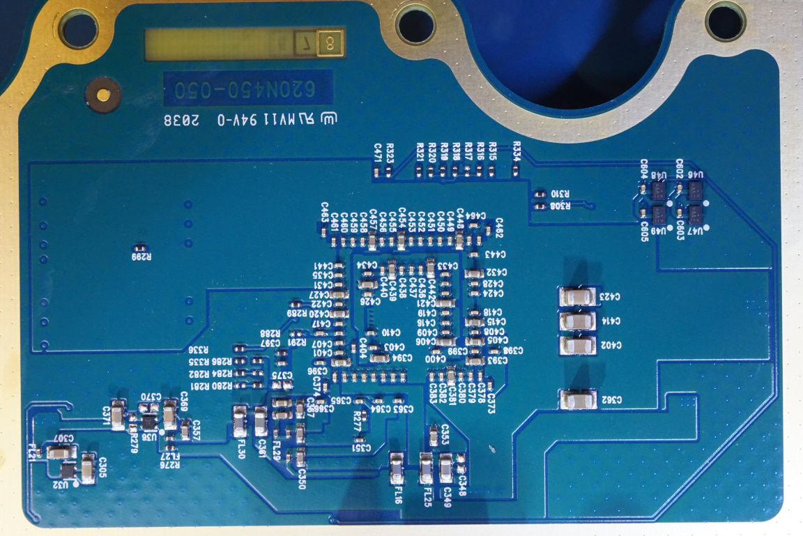
Here is a picture showing the reverse side of the processor section. From the marking on the top, you can also tell this is an 8 layer PCB. In the other picture below you can see an other DC-DC converter section on the reverse side of the board. Here an RT7272A synchronous step-down converter is used. The larger D2PAK device B20200G is an OnSemi’s dual Schottky rectifier.
Because the signal booster has two sets of transceivers that talk to both the cell tower and the cell phones simultaneously, we can expect that the circuitry for these two sections to be relatively similar.
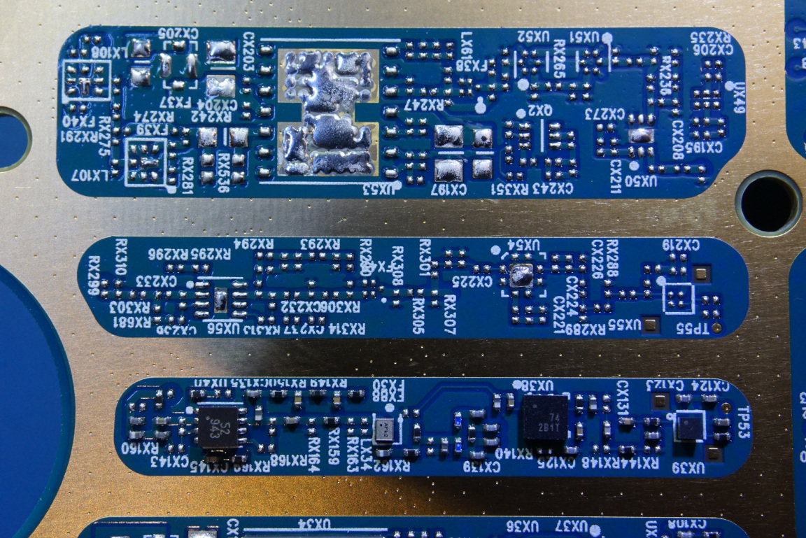
Now we are looking at the downlink section (interfacing broadcasting antenna for the cell phones). You can see a chip marked as 77761-2. This is a Skyworks cellular RF power amplifier specialized for WCDMA applications. The unpopulated footprints again are reserved for other frequency bands for a different model.
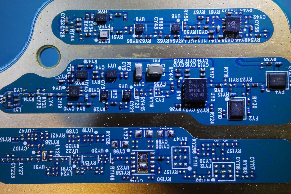
The circuit section shown in the picture below is very similar to the previous section we have seen. This is because this Cel-Fi Go X booster works on both the sub-GHz and 2GHz frequency bands. So it needs two sets of transceivers for the downlink and uplink sections each. Again here you can see another 7761-2 amplifier.
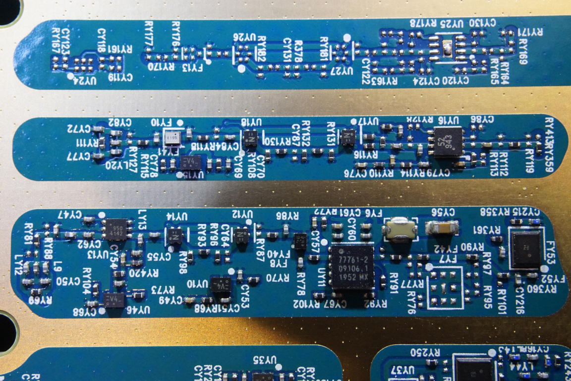
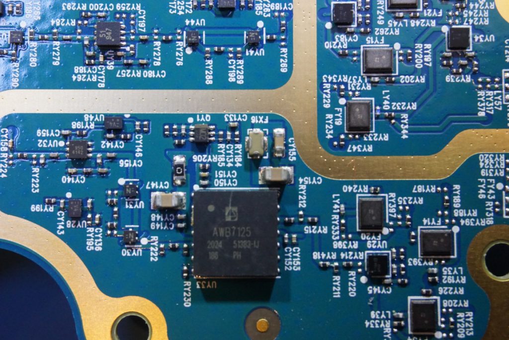
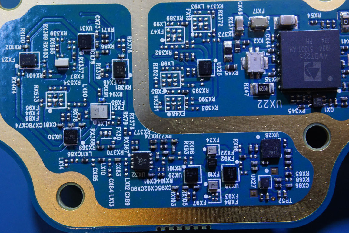
The pictures below highlights the remaining circuitry in the downlink section. Here you can see a Skyworks AWB7125 power amplifier module, which covers the frequency range between 860 MHz and 894 MHz.

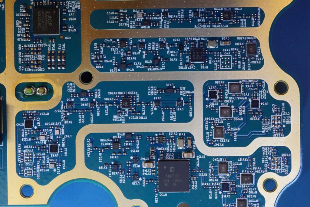
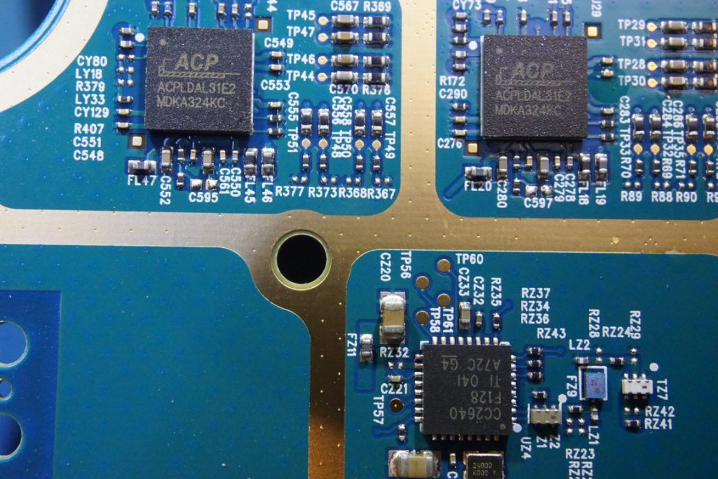
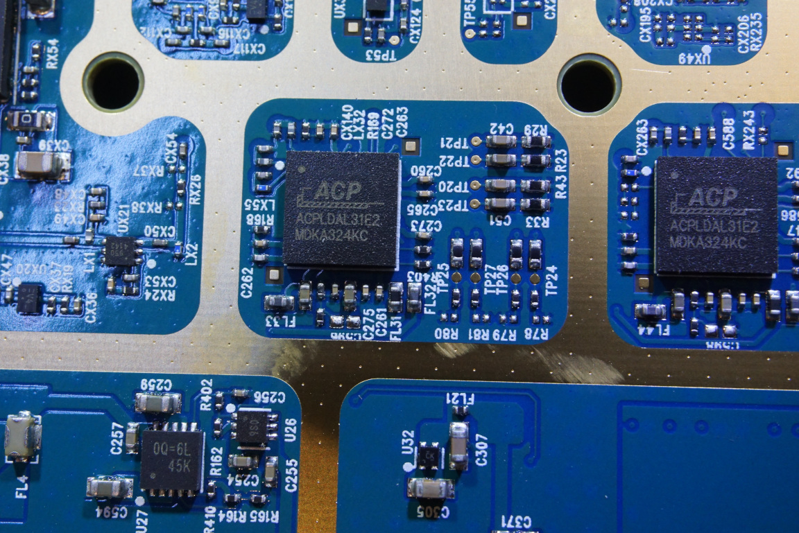
I could not find any information on the ACP chips. Since ACP designs chips for mobile communications, these chips are likely to be some kind of transceivers or DSPs perhaps.
The bluetooth functionality in this signal booster is handled by TI’s CC2640, a 32-bit Arm Cortex MCU.
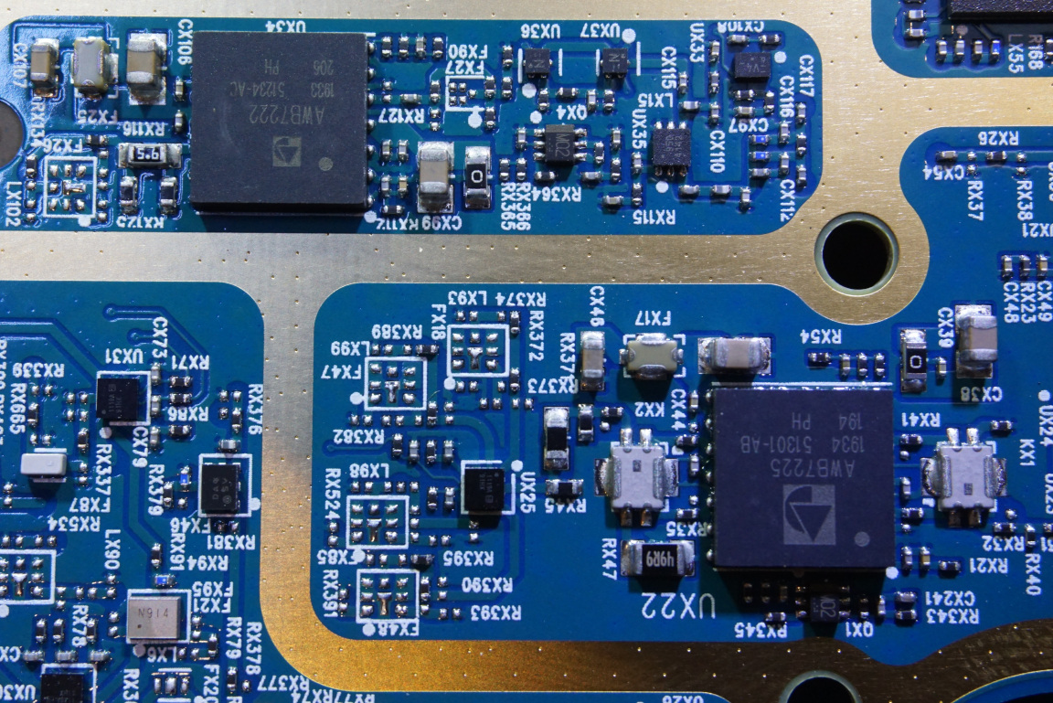
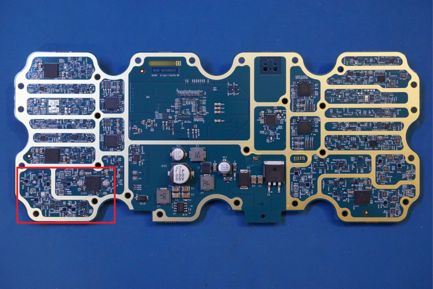
Now moving onto the uplink section which communicates with the cell towers. As mentioned earlier, this section of circuitry bares a lot of resemblance to that of the downlink section.
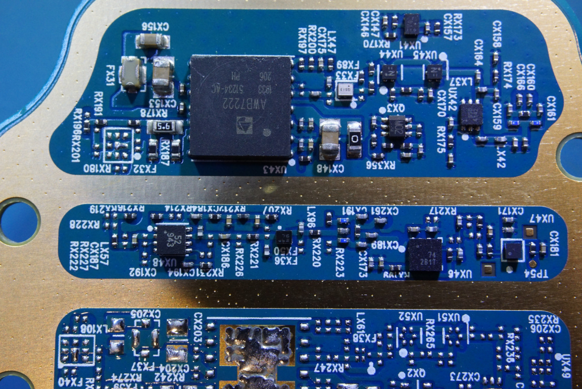
The AWB2222 chip you see here is another Skyworks power amplifier chip, which operates on the 1.805-1.880 GHz frequency band.
Here you can see a couple of unpopulated sections, again these are likely reserved for other frequency bands.
In the picture below, you can see two more Skyworks amplifiers. One is a 7222 for the 1.805-1.880 GHz frequency band. The other is an AWB7225 which covers the 860 MHz to 894 MHz frequency band.
Here is a picture zoomed in to the bottom left of the uplink side of the PCB RF section.
Like the down link section, the uplink section also utilizes two ACP chips.
Below is a video of this teardown.

